
Every standard cell needs a supply voltage and a ground, and every one of them draws current, all at the same time. A power grid is the network of metal that brings VDD and VSS from the chip's supply connections to every cell. It has to do this with very little voltage loss, without wearing out over the chip's lifetime, and while thousands of cells switch at once. This article explains why a dedicated power grid is needed, what can go wrong without a good one, and how much current a small design actually draws.
7 min read | Beginner
What You'll Learn
- Explain why the power network is designed separately from signal routing
- Describe IR drop, electromigration and supply noise in one sentence each
- Estimate the supply current of a design from its power
- List what a power grid must achieve
Current Has to Come From Somewhere
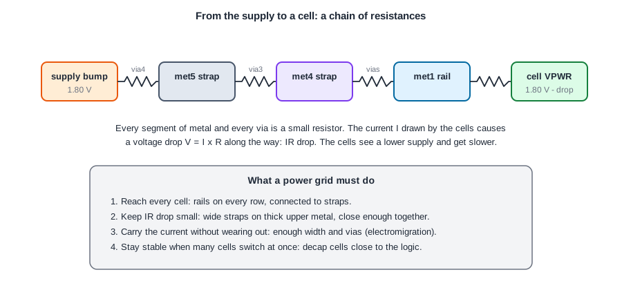
Power reaches a chip through its package: bumps or bond pads connect to the top metal layers. From there the current must flow down through straps, vias and rails to the VPWR pin of every cell, and back from every VGND pin. Each piece of metal and each via is a small resistor. The current through them causes a voltage drop, so the cells see a little less than the supply voltage: this is IR drop, after Ohm's law V = I x R.
A cell with a lower supply is slower. If the drop is large enough, a path that met timing at the nominal voltage fails, or a flip-flop misbehaves. Sign-off flows typically allow a few percent of the supply as total drop, and timing is checked with that lower voltage in mind.
How Much Current?
Power is voltage times current, so the supply current is I = P / V. Two designs from this tutorial, at the typical corner and 1.8 V:
| Design | Power | Average supply current |
|---|---|---|
| 8-bit counter at 200 MHz | 98 uW | 55 uA |
| 16x16 multiplier at 100 MHz, default activity | 3.7 mW | 2.0 mA |
| 16x16 multiplier, inputs toggling 50 % of cycles | 16 mW | 8.9 mA |
A large chip draws amperes. Even in the small multiplier, 8.9 mA has to reach about 1,300 cells spread over 150 um, through rails that are only 0.48 um wide. The average is not the whole story, either: on every clock edge, most flip-flops and the clock tree switch within a fraction of a nanosecond, and the momentary current is many times the average.
Quick Check
Q: A block uses 50 mW at 1.8 V. Its power grid has an effective resistance of 0.2 ohm from the supply to the cells. What is the IR drop, and as a percentage of the supply?
Show Answer
I = 0.05 / 1.8 = 27.8 mA; V = 27.8 mA x 0.2 ohm = 5.6 mV, about 0.3 % of 1.8 V. Real grids are not a single resistor: cells far from the straps see more drop than those close to them.
Three Problems a Grid Must Solve
- IR drop: keep the voltage loss small everywhere, with wide straps on thick upper metal, placed close enough together. See IR Drop.
- Electromigration (EM): a wire that carries too much current per micron of width slowly wears out, over years. Power wires carry the most current, so they need enough width and enough vias. See Electromigration.
- Supply noise: sudden current spikes, together with the inductance of the package, make the supply bounce. Decoupling capacitors (decap cells) close to the logic supply the spikes locally. See Tap Cells, Endcaps and Decaps.
Why the Grid Is Built First
The power grid is built right after the floorplan, before placement and routing, for three reasons:
- It uses the best routing resources, the thick upper layers, and the signal router must work around it.
- The rails define where cells can sit: every row needs its rails.
- It is very hard to add metal to a crowded, routed design. A grid that turns out too weak late in the project forces a large rework.
The power grid is a regular structure: rails along the rows, straps in a fixed pattern, rings around the core and macros. Rails, Rings and Straps describes each part.
Quick Check
Q: Why do flip-flops and the clock network dominate the power of the counter (97 % of it)?
Show Answer
They switch on every clock edge, while most of the counter's logic toggles rarely. The clock net is also the most heavily loaded net in the design. That pattern is common: the clock tree is often a third or more of a block's dynamic power.
Running It in ChipVerify Lab
Run Place and Route on the multiplier and read the Power section of the report: internal, switching and leakage power, and the split between sequential, combinational and clock. Divide the total by 1.8 V to get the average supply current the grid must deliver.
Common Mistakes
Mistake #1: Sizing the grid for the average current
The current peaks on every clock edge. The grid and the decaps must handle the peaks, and the worst-case activity, not just the average of a typical test.
Mistake #2: Leaving the grid until the end
A design routed on a weak grid cannot easily get more power metal later. Plan and check the grid with the floorplan.
Practice Exercise
Challenge: Current per Rail
The multiplier at 16 mW draws 8.9 mA in total. Its core has 56 rows; assume the current splits evenly over them. How much current does each row carry on average, and how does that compare with the met1 limit of 2.8 mA per micron of width for a 0.48 um rail?
Hint
The limit for the rail is its width times the current density limit.
Solution
8.9 mA / 56 = 0.16 mA per row. A 0.48 um met1 rail may carry 0.48 x 2.8 = 1.34 mA, so the average is about 12 % of the limit. The power grid analysis of this design finds the most heavily loaded met1 rail segment at 0.24 mA, still well inside the limit.
Open the ready-made example in the lab, synthesize it and run Place and Route.
Summary
- The power grid brings VDD and VSS from the package to every cell, through straps, vias and rails.
- Its resistance causes IR drop; too much current per width causes electromigration; current spikes cause supply noise.
- Average current is power divided by voltage: 8.9 mA for the multiplier at 16 mW and 1.8 V.
- The grid is built right after the floorplan, on the thick upper layers, before cells and signals.
