
First silicon is the first set of wafers of a new design, and its job is to answer one question as quickly as possible: does the chip work, and if not, what is the cheapest way to fix it? The answer decides whether the design goes to production as it is, needs a metal-only respin that changes only the upper masks, or needs a full respin that starts new wafers from the beginning. This article covers what the first wafers are used for, how teams plan for a fix before tapeout, and which sky130 masks a metal-only fix has to change.
7 min read | Intermediate
What You'll Learn
- Describe what first wafers and corner lots are used for
- Explain wafer holds and why they speed up a fix
- Compare metal-only and full respins and the masks each changes
- Outline the path from first silicon to production
What the First Wafers Are For
The first lot of a new design is an engineering lot. Its dies go to several groups at once:
- Bring-up. Engineers power up the first dies, on a probe station or in a socket on a test board, and check the basics: supply currents, clocks, reset, and the simplest functions. A short or an open in the power grid shows up here in minutes.
- Characterization. Each function is measured across supply voltage, temperature and frequency. A shmoo plot is a common summary: a grid of voltage against frequency, with each point marked pass or fail, showing where the chip works and how much margin it has.
- Correlation. Measured speed is compared with the timing sign-off. The ring oscillators in the scribe lanes and the chip's own critical paths show whether the silicon is faster or slower than the libraries predicted, and whether the margin checked in Post-Route STA was enough.
- Test development. The production test program for wafer sort and final test is debugged on real dies.
- Reliability samples are set aside for qualification, described at the end of this article.
Corner Lots
A single engineering lot comes out somewhere inside the process window, usually near its centre, so it says little about how the design behaves at the edges. Teams therefore often order corner lots, also called split or skew lots: wafers deliberately processed with transistors at the slow and fast ends of the window, matching the corners the libraries were characterized at.
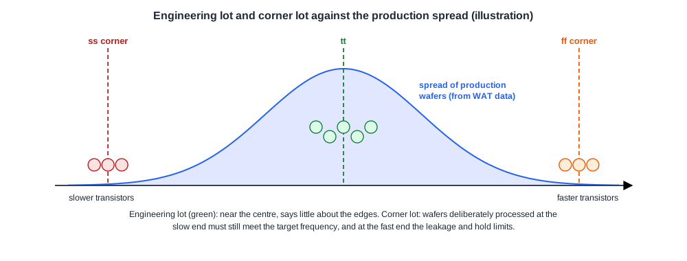
If the slow-corner wafers meet the target frequency and the fast-corner wafers meet the leakage and hold limits, the design has the margin its sign-off claimed. If not, the failing corner points to the fix: more setup margin, or more hold margin, at that corner.
Quick Check
Q: The typical wafers of the first lot run at the target frequency with a little margin. Why is that not enough to release the design to production?
Show Answer
Production wafers will spread across the whole process window, and the slow ones will be slower than the typical ones. Only wafers at the slow corner show whether the design still meets its frequency there, which is what corner lots, or a careful correlation of typical silicon with the slow-corner timing, are for.
Planning for a Fix Before Tapeout
Two decisions made before tapeout decide how fast a bug can be fixed later.
Spare cells. As described in ECOs After Routing, unconnected gates and flip-flops spread over the core let a logic fix be built by rewiring alone. Some libraries also provide ECO cells that occupy filler positions and can be turned into logic gates by changing only the upper layers.
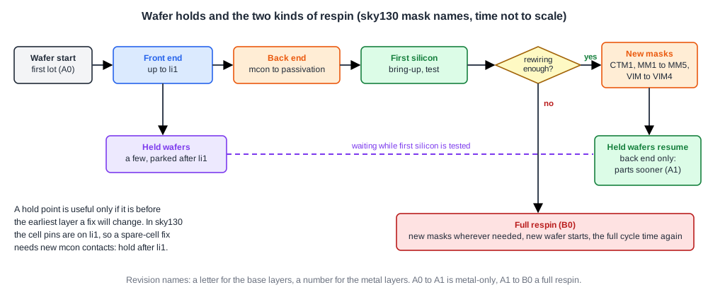
Wafer holds. When the first lot starts, a few of its wafers are stopped part way through the process, just before the first layer a fix would be likely to change. If first silicon finds a bug that rewiring can fix, the held wafers continue with the new masks and finish in a fraction of the full cycle time. If not, they are released unchanged.
Which Masks a Metal-Only Fix Changes
A "metal-only" fix changes the wiring, not the transistors. Which masks that means depends on the process. In sky130 the standard cell signal pins are on li1, the local interconnect: the nand2 cell's A, B and Y pins are li1 shapes, and every routed connection reaches them through an mcon contact, 42,667 of them in the flattened multiplier. A new connection to a spare cell therefore needs a new mcon as well as new metal.
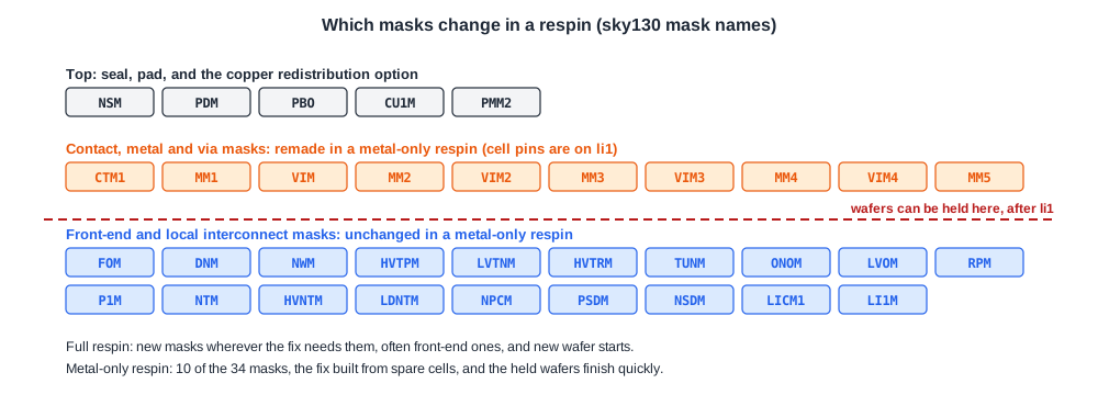
So a metal-only respin in sky130 remakes 10 of the 34 masks, the contact mask CTM1, the five metal masks and the four via masks, and the wafers must be held after li1, before the mcon contacts. The other 19 masks below, from FOM to LI1M, and the wafers processed with them, stay as they are.
A fix that changes a transistor, adds a cell where no spare exists, or resizes a cell changes the front-end masks too, and is a full respin. Resizing is easy to mistake for a wiring change: the lab's ECO run that resized 18 cells, in ECOs After Routing, changed the cells' diffusion and poly as well, so on real silicon it would have needed front-end masks.
Quick Check
Q: A team holds its wafers before met1, expecting to do metal-only fixes. In a process where the cell pins are on li1, why might the held wafers be useless for a spare-cell fix?
Show Answer
Connecting a spare cell needs new contacts from li1 up to met1, and those contacts are made before met1. Wafers held after the contact step already have the old contacts and cannot get the new ones. The hold point must be before the earliest layer a fix will change, here before the mcon contacts.
Full Respin or Metal-Only
| Metal-only respin | Full respin | |
|---|---|---|
| What can change | wiring, using spare and ECO cells | anything |
| Masks (sky130) | 10 of 34 | as many as the fix touches, up to all |
| Wafers | held wafers continue | new wafer starts |
| Time | back-end part of the cycle time | the full cycle time again |
| Cost | mostly the cheaper upper masks | includes the critical front-end masks |
Many companies name their mask revisions so that the difference is visible: a letter for the base layers and a number for the metal layers, so that A0 to A1 is a metal-only respin and A1 to B0 a full one.
Failure Analysis
When a die fails and the cause is not obvious from the design, failure analysis finds it physically. Emission microscopes and laser scanning locate the spot where current flows that should not, and a focused ion beam (FIB) cuts a cross-section through it for an electron microscope. The same FIB can also edit a circuit: cut a wire or deposit a new connection on a few dies, to prove a fix works before paying for masks.
From First Silicon to Production
- Qualification. Samples are stressed at high temperature and voltage for long periods, cycled in temperature, and tested for electrostatic discharge and latch-up, to show the part will last its intended lifetime.
- Risk production. The first production wafers run before qualification completes, to shorten time to market.
- Ramp. Volume increases while yield learning lowers the defect density and the test program is shortened, both lowering the cost per part, as Yield and the Cost of a Good Die showed.
Running It in ChipVerify Lab
Run Place and Route on the multiplier, download the GDSII and open any standard cell: its signal pins are on li1, and the router's wires reach them through mcon contacts. With PRO, an ECO run with a replace_cell command shows a change that would be a full respin, because the replacement cell has different transistors; a change that only adds wires between existing cells would be the metal-only kind.
Common Mistakes
Mistake #1: Holding wafers at the wrong layer
The hold point must be before the earliest layer a fix will change, which depends on where the cell pins are.
Mistake #2: Calling a resize a metal-only fix
A different drive strength is a different cell, with different transistors. Only rewiring is metal-only.
Mistake #3: Judging margin from typical wafers
Typical silicon hides corner failures. Use corner lots or correlate carefully with the slow and fast corners.
Practice Exercise
Challenge: Classify the Fixes
First silicon shows three problems: (a) a missing inversion on an enable signal, with a spare inverter 20 um away; (b) a path that fails at the slow corner by 0.3 ns and would close if two cells were upsized; (c) a short between two met2 wires caused by a layout error. For each, say whether it can be a metal-only respin in sky130, and which masks it changes.
Hint
Ask whether any transistor changes, and whether a new connection reaches a cell pin on li1.
Solution
(a) Metal-only: the spare inverter is connected with new wiring, which needs new mcon contacts to its li1 pins, so CTM1 and the metal and via masks change. (b) Not metal-only: upsizing replaces cells with different transistors, a full respin unless a spare cell can take over the path, for example a spare buffer used to split the load. (c) Metal-only: rerouting the met2 wires changes MM2 and perhaps the vias around it, with no front-end change.
Open the ready-made example in the lab, synthesize it and run Place and Route.
Summary
- First silicon is used for bring-up, characterization, correlation with timing sign-off, test development and reliability samples.
- Corner lots processed at the slow and fast ends of the window show whether the design has the margin its sign-off claimed.
- Spare cells and wafer holds, planned before tapeout, make metal-only fixes fast.
- In sky130 the cell pins are on li1, so a metal-only respin remakes 10 of 34 masks: CTM1, the metal and the via masks, with wafers held after li1.
- Resizing or adding transistors is a full respin; failure analysis and FIB edits find and prove fixes before masks are bought.
