
The antenna effect is damage that happens to a transistor gate while the chip is still being manufactured. During plasma etching of each metal layer, a long wire collects electric charge. If that wire is connected only to a gate, the charge has nowhere to go except through the gate's thin oxide, and the oxide can be weakened or destroyed before the chip is ever powered. This article explains the mechanism, the antenna ratio rules in the sky130 LEF, how to read OpenROAD's antenna report, and the two fixes: antenna diodes and layer jumps.
7 min read | Intermediate
What You'll Learn
- Explain why long wires damage gate oxide during manufacturing
- Calculate an antenna ratio and compare it with the sky130 limit
- Read the antenna report from
check_antennas - Choose between a diode and a layer jump to fix a violation
Charge Collected During Manufacturing
Metal layers are built one at a time from the bottom up. Each one is deposited and then etched in a plasma, a gas of charged particles. Exposed metal picks up charge from the plasma, and the longer the wire, the more charge it collects.
Once the chip is finished, every net has a driver, and the driver's source and drain diffusions give charge a safe path into the substrate. During manufacturing that path may not exist yet. While met3 is etched, met4 and met5 are not built, so a net whose connection to its driver goes up through met4 is split in two: the gate side and the driver side are not yet joined.
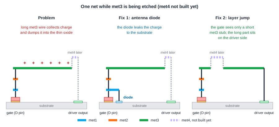
If the gate side holds a long met3 wire, all the charge it collects flows into the gate. The gate oxide in sky130 is a few nanometres thick, so a small charge creates a large field across it. The result is either immediate breakdown or a weakened oxide that shifts the transistor's threshold voltage and fails early in the field.
The effect is cumulative per layer: what matters is the metal connected to the gate at the moment each layer is etched. Wires on layers above that are not there yet, and once a layer connects the gate to a diffusion, the net is safe for every layer after it.
Antenna Ratios
Foundries express the rule as a ratio: the area of metal connected to a gate, divided by the area of that gate. The technology LEF gives the limits per layer, and the cell LEF gives each input pin's gate area. For sky130 the metal layers use the side area of the wire, the area of its sidewalls, because charge is collected mainly at the edges during etching:
LAYER met3
  THICKNESS 0.8 ;
  ANTENNAMODEL OXIDE1 ;
  ANTENNADIFFSIDEAREARATIO PWL ( ( 0 400 ) ( 0.0125 400 ) ( 0.0225 2609 ) ( 22.5 11600 ) ) ;
The limit is a piecewise-linear table of the diffusion area connected to the net. With no diffusion on the gate side, the allowed ratio is 400. As soon as a diode or other diffusion of more than 0.0225 um2 is connected, the limit jumps to thousands, because the diffusion drains the charge.
A D input of sky130_fd_sc_hd__dfxtp_1 has a gate area of 0.126 um2. A ratio of 400 allows 400 x 0.126 = 50 um2 of met3 sidewall. A met3 wire 0.8 um thick has two sidewalls, 1.6 um2 per micrometre of length, so the limit is reached at about 31 um of met3 on the gate side with nothing else to drain it.
Quick Check
Q: A long met3 wire connects to a gate through met1 and met2 only, and the driver connects to the same met3 wire through met1 and met2 on the other side. Is the gate at risk while met3 is etched?
Show Answer
No. While met3 is etched, the met3 wire already joins the gate and the driver, so the driver's diffusion drains the charge. The risk exists only when the connection to a diffusion is completed on a higher layer that is not yet built.
Reading the Antenna Report
The lab's flow runs check_antennas after detailed routing and writes antenna.rpt. The 16x16 multiplier at 44 % utilization has no violations, so this example uses a different design: a 32 x 16 register file whose 32 rows each have their own clock gating cell, routed at 50 % utilization without antenna repair. The log reports:
[INFO ANT-0002] Found 12 net violations.
[INFO ANT-0001] Found 12 pin violations.
The report lists every pin of every violating net, layer by layer. The worst one, shortened:
Net: _0011_
  Pin:   _1591_/D (sky130_fd_sc_hd__dfxtp_1)
    Layer: met2
      Partial area ratio:   20.19
      Required ratio:  400.00 (Side area)
      Cumulative area ratio:   53.64
    Layer: met3
      Partial area ratio:  993.21
      Required ratio:  400.00 (Side area) (VIOLATED)
      Cumulative area ratio: 1046.85
- Partial area ratio is the ratio for this layer alone. On met3 it is 993.21, almost 2.5 times the limit of 400.
- Required ratio is the limit for this layer. A value of 0.00 means the rule is not checked; sky130 sets limits on the side area of metals and on the area of vias.
- Cumulative area ratio adds up the layers below. sky130 does not check it.
Working backwards: 993.21 x 0.126 = 125 um2 of met3 sidewall, or about 78 um of met3 connected to the D pin while met3 is etched.
The 12 violating nets were spread over the design:
| Gate pin type | Nets | Layer | Worst ratio |
|---|---|---|---|
| D input of a flip-flop | 3 | met3, met1 | 993.21 |
| GATE input of a clock gating cell | 5 | met3 | 789.28 |
| Inputs of logic gates | 3 | met3, met1 | 762.35 |
| CLK input of a flip-flop | 1 | met1 | 415.16 |
Eight of the twelve are on met3, where long horizontal routes run, and the rest are on met1. Each one is a long wire on the gate side of the net at the moment the layer is etched.
Fix 1: Antenna Diodes
An antenna diode is a small cell that contains only a reverse-biased diffusion. Connected to the net next to the gate, it gives the charge a path to the substrate during manufacturing. In normal operation it is reverse biased and only adds a little capacitance and leakage. In sky130 it is sky130_fd_sc_hd__diode_2, with a diffusion area of 0.4347 um2, which lifts the met3 limit for the gate from 400 to about 2,774.
OpenROAD inserts diodes with repair_antennas, which runs after global routing: it finds the violating nets from the route guides, places a diode next to each affected pin and updates the routing. To do that it must know which cell is the diode, and it recognizes the diode by its LEF class, CORE ANTENNACELL, and by the ANTENNADIFFAREA of its pin.
In the sky130 cell LEF as the library ships it, the diode has neither, so repair_antennas stops with a warning and changes nothing; the 12 violations above are what was left after that step:
[WARNING GRT-0246] No diode with LEF class CORE ANTENNACELL found.
Quick Check
Q: Why is the diode placed next to the gate pin, and not next to the driver?
Show Answer
The danger is on the gate side of the net, the part that is not yet connected to the driver while a layer is etched. A diode near the driver would sit on the other part of the split net and would not drain the charge collected by the wire attached to the gate.
Fix 2: Layer Jumps
The other fix changes the routing instead of adding a cell. If the long met3 wire is broken near the gate and finished with a short hop up to met4 and back down, the gate side only carries a short met3 stub while met3 is etched. The long part of the wire sits on the driver side, which is safe. When met4 is built, the two parts join, and by then the gate is connected to the driver's diffusion.
A layer jump costs two vias and a little met4, but no cell area. It works best when the violation is on a lower layer and the layer above has free tracks. OpenROAD's repair_antennas can insert jumpers as well as diodes.
Two more fixes appear in practice. A buffer inserted near the gate splits the net into two shorter nets, each with its own driver. And routing a long net on the top layers avoids the problem, since the higher the layer, the more of the net is already connected when it is etched.
Repair in Practice
To see the repair work, the same register file was routed again with the cell LEF from OpenROAD-flow-scripts, where diode_2 has class CORE ANTENNACELL and its diffusion area. This time the repair step reported:
[INFO GRT-0302] Inserted 7 jumpers for 7 nets.
[INFO ANT-0002] Found 3 net violations.
[INFO ANT-0001] Found 3 pin violations.
- Jumpers first. The repair fixed 7 nets with layer jumps and inserted no diodes. The cell area stayed at 17,295 um2 and the worst setup slack moved by 0.01 ns.
- New violations after detailed routing.
check_antennasstill found 3 violations, all on met1 at flip-flop inputs, with ratios from 420 to 547. Two of them were not in the first list.
The reason is the order of the steps. repair_antennas runs on the global routes, which are only an estimate of the final wires. The detailed router then draws the real met1 segments, and some of them turn out longer. OpenROAD-flow-scripts therefore runs repair_antennas a second time after detailed routing, followed by an incremental detailed route, and only then the final check. The lab's flow does the same, and repeats the repair and incremental route up to three times while the count keeps falling.
Running It in ChipVerify Lab
Run Place and Route on the multiplier and open the Antenna section of the report. The lab's cell LEF marks sky130_fd_sc_hd__diode_2 as CORE ANTENNACELL with its diffusion area, and the flow repairs after global routing and again, up to three times, after detailed routing. At 40 % the multiplier had 3 violations after global routing; the repair inserted 3 diodes and one jumper, and the final check is clean.
The clock-gated register file shows the two passes at work (a PRO run, since it takes about nine minutes). The first repair fixed 21 nets with 3 jumpers and 21 diodes. Detailed routing then created 4 new violations, the second repair added 4 more diodes, and the final check is clean. In an earlier run of the same design one violation survived both passes, a met4 ratio of 608 on the GATE pin of a clock gate; a violation like that is fixed by hand, with a diode or a reroute, before tapeout.
Common Mistakes
Mistake #1: Treating antenna violations as harmless warnings
A layout with antenna violations can pass simulation and timing and still come back from the fab with damaged or slowly degrading transistors. Foundries reject designs that fail the antenna rules.
Mistake #2: Placing the diode far from the gate
The diode must be on the gate side of the split net, close to the pin. Placed elsewhere, it may be on a different piece of metal when the critical layer is etched.
Mistake #3: Fixing every violation with diodes
Each diode adds area, capacitance and leakage. Where tracks are free, a layer jump or a reroute fixes the same violation without a cell.
Practice Exercise
Challenge: How Long Can the Wire Be?
The GATE input of sky130_fd_sc_hd__dlclkp_1 has a gate area of 0.159 um2. In sky130 met3 is 0.8 um thick and the side area limit is 400 without a diode. What is the longest met3 wire that can be connected to this pin alone while met3 is etched? One such net reported a ratio of 789.28; about how long was its met3 wire?
Hint
Side area per micrometre of wire is twice the thickness.
Solution
Allowed side area: 400 x 0.159 = 63.6 um2. At 1.6 um2 per micrometre, the wire may be about 40 um long. The violating net had 789.28 x 0.159 = 125.5 um2, about 78 um of met3, roughly twice the limit.
Open the ready-made example in the lab, synthesize it and run Place and Route.
Summary
- Plasma etching charges long wires; if a wire reaches only a gate when its layer is etched, the charge flows through the thin gate oxide.
- The rule is a ratio of connected metal area to gate area; for sky130 metals it uses side area with a limit of 400 when no diffusion is connected.
check_antennaslists each violating pin with the partial ratio per layer; a clock-gated register file routed without antenna repair had 12 violations, most on met3.- An antenna diode near the gate drains the charge and raises the limit; a layer jump keeps the long wire on the driver side instead.
- Repair runs on global routes, so a second repair after detailed routing catches the violations the real wires create.