
The package is the bridge between the die and the circuit board. It carries every signal and supply, removes the heat, and protects the silicon. It is no longer possible to separate the design of a high-performance chip from the design of its package. Chip-package co-design means making die and package decisions together: which package, which side each signal leaves on, how many supply connections, and how much power the package can carry away. This article walks through the path from die to board, the parasitics and thermal limits along it, and how they shape the physical design.
7 min read | Intermediate
What You'll Learn
- Trace a signal and a supply from the die through the package to the board
- Describe the parasitics a package adds
- Calculate a chip's power limit from thermal resistance
- List the decisions die and package designers make together
From Die to Board
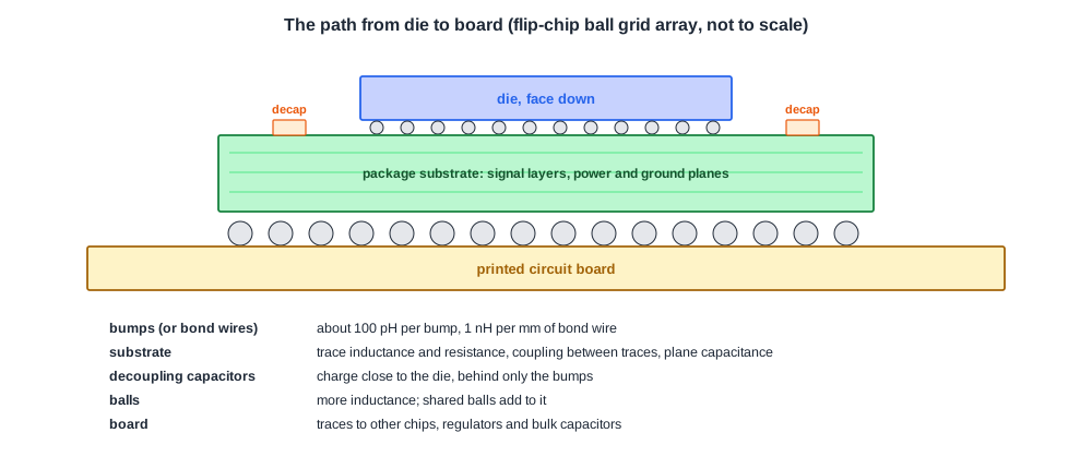
An ideal package does four things: connect signals and power with little delay or distortion, remove heat, protect the chip from mechanical damage and thermal expansion stress, and be cheap to manufacture and test. Each connection passes several stages:
- Die to package. Bond wires from edge pads, or solder bumps over the die, as in Flip-Chip: Bump Maps and RDL Routing.
- Through the package. A lead frame in simple packages; in advanced ones a substrate that internally resembles a printed circuit board, with signal layers, power and ground planes, and controlled-impedance lines.
- Package to board. Leads, solder balls or lands.
Common package families range from leaded quad flat packs with 44 to 240 pins on the edges, through ball grid arrays with balls under the whole package, to chip-scale packages no larger than 1.2 times the die. Caravel's documented package is a wafer-level chip-scale package with 60 balls at 0.5 mm pitch.
What the Package Adds
Every stage adds parasitics. A package model has inductance in the bond wires and lead frame, mutual inductance and capacitance between neighbouring signals, and resistance in the supply paths, which matters at large currents. Typical figures for the largest term, the die connection, are about 1 nH per millimetre of bond wire and about 100 pH per solder bump.
The effects reach back into the chip:
- Supply noise. Package inductance in the supply path causes the ground bounce and droop of Power and Ground Pads: How Many and Where.
- Crosstalk. Neighbouring bond wires and package traces couple to each other, so fast signals need ground connections between them.
- Signal timing. The package trace adds delay and, at high speeds, reflections if its impedance does not match the board and the driver.
- Decoupling. High-performance packages include capacitors between supply and ground close to the die. One example is a processor in a land grid array package with 1,366 lands and an array of bypass capacitors on the back of the substrate, directly opposite the die.
Quick Check
Q: Why do capacitors on the package substrate help with supply noise that the board's capacitors cannot reduce?
Show Answer
The noise comes from fast current changes through the inductance between the die and the capacitor. A capacitor on the substrate is separated from the die by only the bumps or bond wires, while a board capacitor also sits behind the package balls and traces. Less inductance between the die and the charge store means less voltage for the same dI/dt.
Heat
The package is also the heat path. The junction temperature rise is:
temperature rise = thermal resistance (junction to ambient) x power
thermal resistance = junction-to-package + package-to-ambient
Typical figures show how much the package and cooling matter. Still air removes about 0.001 W per cm2 per degree, so a package with 10 cm2 of surface has about 100 °C/W and cannot handle much more than 1 W. A 72-pin ceramic package measures 34 °C/W in still air and 10 °C/W with airflow and a good heat sink.
A worked example: a ball grid array with 0.9 °C/W from junction to package, a heat sink with 4.0 °C/W plus 0.1 °C/W of adhesive, an ambient of up to 55 °C, and a junction limit of 100 °C. The total is 5 °C/W, the allowed rise is 45 °C, so the chip may dissipate at most 9 W.
For the physical designer, the thermal limit is a power budget, and the power analysis of the floorplan must stay inside it. Hot spots matter too: a block with a high power density raises the local temperature, which slows its cells and raises leakage, so very hot blocks are spread out or placed where the package removes heat best.
Decisions Made Together
Die and package designers agree on:
- Package type and size, from the pin count, the power, the board technology and the cost.
- The ballout: which signal and supply goes to which ball, often fixed early by the board designers who will use the chip.
- Pad or bump order on the die, which must allow the package to route from every pad to its ball without crossings it cannot make. A signal whose ball is on the north side should not have its pad on the south side.
- Supply connections: how many pads, bumps and balls for each supply, and whether several pads share a ball. Caravel's documented ballout puts its grounds vssio, vssa and vssd on four shared balls.
- Die size and keep-outs: the package cavity or bump field fixes the allowed die outline, and bond wire angles limit how close pads can be to the corners.
- Thermal budget, as above.
The usual working method is iterative. The chip team proposes a pad order from its floorplan, the package team routes the substrate and reports what cannot be routed or what parasitics result, and both adjust. Because the die's pad ring and the package substrate are designed in different tools, the pad list with coordinates is the shared contract, kept under version control like the netlist.
Quick Check
Q: The board team fixes the ballout before the floorplan exists. Which part of the physical design does this constrain most?
Show Answer
The pad ring and the top-level floorplan. Each signal must reach the side of the die near its ball, so the pad order is largely fixed, and the blocks that use each interface should then be placed near those pads to keep the top-level routes short.
Running It in ChipVerify Lab
At the time of writing, the lab works on blocks and has no package model. Its power report, described in Power Sign-Off: IR Drop and EM, gives the power that the thermal calculation needs: multiply it by a package's thermal resistance to estimate the temperature rise. For a small block the result is tiny; the method is the same for a full chip.
Common Mistakes
Mistake #1: Choosing pad order without the package router
A pad order that looks good on the die can be impossible to route in the substrate. Agree on it with the package designer.
Mistake #2: Ignoring the thermal budget until sign-off
The package limits the chip's power. Check the power estimate against it during floorplanning.
Mistake #3: Sharing supply balls freely
Each shared ball adds inductance to the supplies on it. Share only supplies that can tolerate it, such as grounds of the same domain.
Practice Exercise
Challenge: Power Budget
A chip in a package with 30 °C/W from junction to ambient may reach a junction temperature of 105 °C in an ambient of 45 °C. What is its power limit? If a heat sink brings the total to 12 °C/W, what is the new limit?
Hint
Allowed rise divided by thermal resistance.
Solution
The allowed rise is 105 - 45 = 60 °C. Without the heat sink: 60 / 30 = 2 W. With it: 60 / 12 = 5 W. The heat sink more than doubles the power the chip may use.
Summary
- The package connects die to board, removes heat and protects the chip; its design cannot be separated from the chip's.
- Bond wires add about 1 nH per millimetre and bumps about 100 pH; package inductance and coupling affect supply noise, crosstalk and timing.
- Temperature rise is thermal resistance times power; for example, 9 W is allowed at 5 °C/W and a 45 °C rise.
- Package type, ballout, pad order, supply connections, die outline and thermal budget are decided jointly.
- The pad list with coordinates is the contract between die and package design.
