
The front-end of line (FEOL) is the part of fabrication that builds the transistors in the silicon: the wells, the isolation between devices, the gate oxide and gate, and the doped source and drain regions. It ends with the first contacts that connect the transistors to the wiring above. Every one of these steps is defined by a mask, and every mask comes from layers that a standard cell library drew. This article walks through a typical CMOS front-end sequence and maps each step to the sky130 layers found in the GDSII of the routed multiplier from the lab.
7 min read | Intermediate
What You'll Learn
- List the front-end steps of a CMOS process in order
- Explain the self-aligned gate and why spacers exist
- Map each step to the sky130 drawn layers and masks
- Connect front-end steps to design rules seen earlier in this tutorial
The Inverter in Cross-Section
The picture below is the inverter of every standard cell, cut through its two transistors. The labels give the sky130 drawn layer behind each part; the numbers in the caption come from the process assumptions in the sky130 PDK documentation.
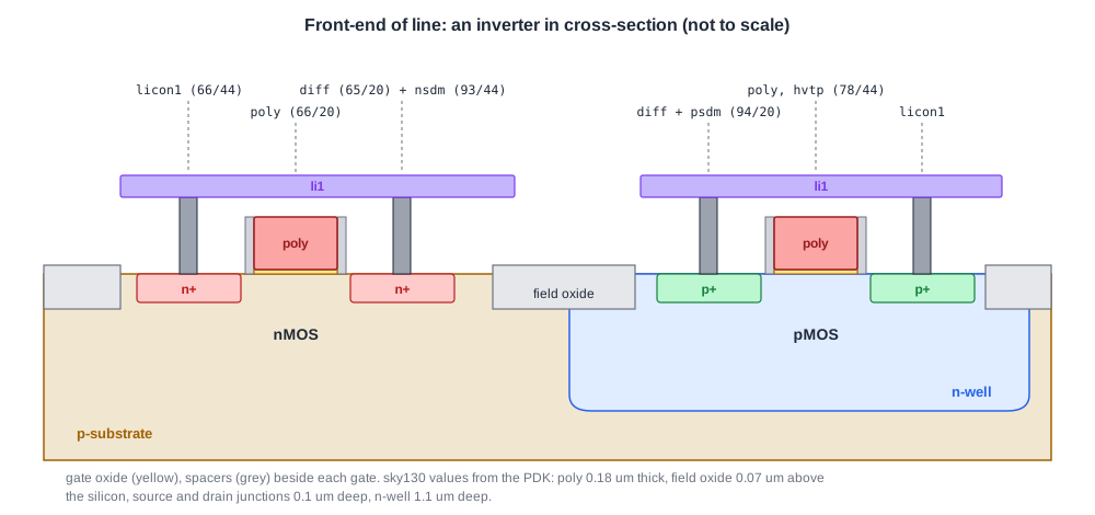
The nMOS sits directly in the lightly doped p-type substrate, or in a p-well. The pMOS sits in an n-well. The steps below build this structure from the bottom up.
1. Wells
The first masks define the wells. Dopant ions are implanted where the resist is open, and a high-temperature anneal activates them and lets them spread. Modern wells are often retrograde, implanted at high energy so that the doping peaks below the surface, which improves latch-up resistance. In sky130 the n-well is about 1.1 um deep and the p-well about 0.75 um.
In the multiplier's GDSII the n-well layer (64/20) has 4,040 shapes, one in each cell instance, the same number as the standard cell area markers. In a row of abutted cells these shapes touch and form one continuous n-well strip along the row, which is why the cell library puts the n-well at the same height in every cell. The taps that bias these wells, discussed in Tap Cells, Endcaps, Latch-Up and Decaps, are the 638 shapes on the tap layer (65/44).
2. Threshold Implants
Extra implants set the threshold voltage of each transistor type. A process with several threshold options needs one mask per option, which is why multi-Vt libraries cost masks. The sky130 mask list includes High Vt PCh (HVTPM) and Low Vt Nch (LVTNM) masks. The multiplier's GDSII has 4,044 shapes on the hvtp layer (78/44): the pMOS transistors of the sky130 high-density library use the high-threshold option, as described in Multi-Vt Cells and Leakage.
3. Isolation
Neighbouring transistors must not interact, and a wire crossing the silicon must not create a parasitic transistor under it. Thick oxide between the active areas provides this isolation. Older processes grew it by local oxidation, which spread sideways into a "bird's beak"; since around 0.35 um most processes etch shallow trenches around the active areas, fill them with oxide and polish the surface flat (shallow trench isolation).
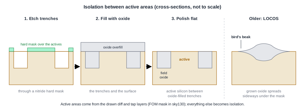
The drawn layers are the active areas: diff (65/20) for transistors and tap (65/44) for well and substrate contacts. The mask that patterns them is called Field Oxide (FOM) in sky130, whose PDK gives the field oxide 0.07 um above the silicon surface. Everything outside diff and tap becomes isolation.
Quick Check
Q: In a GDSII, poly that crosses diff forms a transistor, but poly that runs over the area between diffs does not. What process step makes this true?
Show Answer
Isolation. Outside the drawn active areas the silicon is covered by thick field oxide, so poly over it is far from the silicon and cannot invert a channel at normal voltages. Only where poly crosses an active area does it sit on thin gate oxide over silicon and form a transistor.
4. Gate Oxide and Gate
A very thin, high-quality oxide is grown on the active areas, then polysilicon is deposited over the whole wafer and patterned with the poly mask (P1M, from the drawn poly layer 66/20). The poly forms both the transistor gates and short poly wires. In sky130 the poly is 0.18 um thick.
Many processes offer two oxide thicknesses: thin oxide for the core logic and thick oxide for higher-voltage I/O transistors. sky130 has 1.8 V core devices and 5 V devices, and a Low Voltage Oxide mask (LVOM) in its list. A design that uses only core cells, like the multiplier, has no shapes for the thick-oxide option.
Advanced nodes replace the poly and oxide with a high-k dielectric and a metal gate, but the sequence of defining the gate before the source and drain is the same.
5. Source and Drain, Self-Aligned
The gate is patterned before the source and drain are implanted, and it blocks the implant beneath it. The source and drain therefore line up exactly with the gate edges, whatever small misalignment the mask had. This self-aligned gate is what makes short, fast transistors possible.
The implant happens in two stages:
- Tip implants. A light, shallow implant next to the gate (the lightly doped drain) reduces the electric field at the drain. sky130's mask list includes N-tip implant masks (NTM, HVNTM, LDNTM); a block GDSII has no layer for them, because they are derived from the drawn layers or belong to other devices.
- Spacers and the deep implant. Thin insulating spacers are formed on both sides of the gate (0.05 um in the sky130 assumptions), and a heavy implant then forms the deep source and drain outside them. The N+ Implant (NSDM) and P+ Implant (PSDM) masks come from the drawn nsdm (93/44) and psdm (94/20) layers, 4,359 shapes each in the multiplier. In sky130 the junctions are about 0.1 um deep.
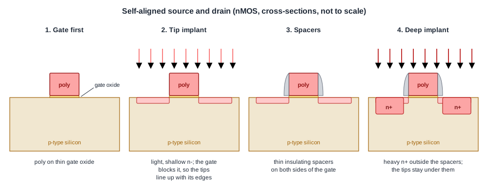
A final anneal activates the dopants. After this, the process keeps temperatures low so that the junctions do not move.
6. Contacts and Local Interconnect
A dielectric is deposited over the transistors and polished flat (0.5 um before the local interconnect in sky130). Contact holes are etched through it to the source, drain and gate regions and filled with a conductor. In sky130 these are the licon1 contacts (66/44), 27,221 of them in the flattened multiplier, landing on li1, a thin local interconnect layer (67/20) below met1 that the cells use for their internal wiring. The npc layer (95/20), "Nitride Poly Cut" in the mask list, marks the poly areas where licon contacts land.
This boundary between transistors and wires is sometimes called the middle of line. Above it begins the back-end of line, covered in Back-End-of-Line and Wafer Out.
Quick Check
Q: Why does the process implant the source and drain after patterning the gate, rather than before?
Show Answer
So the gate itself acts as the implant mask. The source and drain then end exactly at the gate edges, with no overlap or gap from mask misalignment. Implanting first would require the gate to overhang the source and drain by the alignment tolerance, adding capacitance and slowing the transistor.
Why Front-End Rules Look the Way They Do
- Poly extension past diff exists because the gate must cover the full channel width even if the poly end prints short.
- Implant enclosure of diff exists because the nsdm and psdm masks are aligned separately and must still cover the whole active area.
- Tap spacing exists because the well resistance between a transistor and its tap decides latch-up risk.
- Antenna ratios, from The Antenna Effect and Diode Insertion, protect the thin gate oxide built in step 4 from the charge of plasma etches later in the back end.
Running It in ChipVerify Lab
Run Place and Route on the multiplier, download the GDSII and open one standard cell, such as an inverter, in KLayout. Turn on nwell, diff, tap, poly, nsdm, psdm, hvtp, licon1 and li1 one at a time and find each part of the cross-section above: the n-well over the pMOS half, poly crossing diff for each transistor, the implant layers covering the active areas, and the licon contacts landing on li1.
Common Mistakes
Mistake #1: Reading poly over field oxide as a transistor
Only poly crossing an active area forms a gate. Elsewhere poly is a wire.
Mistake #2: Treating implant layers as optional decoration
Missing nsdm or psdm leaves a transistor without proper source and drain. LVS extracts device types from these layers.
Mistake #3: Mixing threshold options without knowing the mask cost
Each threshold option is an extra mask and implant. A library choice is also a process choice.
Practice Exercise
Challenge: Masks for One Transistor
The sky130 PDK's device table lists, for a standard 1.8 V nMOS, three masks that are created for the device: FOM, P1M and NSDM. Which front-end step does each one pattern, and which drawn layer in the multiplier's GDSII does each come from? Why is NWM not in the list?
Hint
Follow steps 3, 4 and 5 above, and remember where the nMOS sits.
Solution
FOM patterns the active areas and isolation (step 3), from diff and tap. P1M patterns the gate (step 4), from poly. NSDM masks the N+ source and drain implant (step 5), from nsdm. NWM is not needed because the nMOS sits in p-type silicon, outside the n-well; the pMOS needs NWM and PSDM instead.
Open the ready-made example in the lab, synthesize it and run Place and Route.
Summary
- The front end builds wells, threshold implants, isolation, gate oxide and gate, source and drain, then contacts.
- The self-aligned gate uses the patterned poly as the implant mask, so source and drain match the gate edges.
- Spacers separate the light tip implant from the deep source and drain implant.
- In the lab multiplier, nwell, diff, tap, poly, hvtp, nsdm, psdm, licon1 and li1 carry the front-end shapes; each matches a sky130 mask.
- Front-end rules such as poly extension, implant enclosure, tap spacing and antenna ratios follow from these steps.