
A chip is built on a wafer, a thin disk of single-crystal silicon, inside a cleanroom where the air holds almost no particles. Every layer of the chip is defined by lithography: the wafer is coated with photoresist, exposed through a mask field by field, developed, and then etched or implanted where the resist is open. This cycle repeats once for every mask layer, so a chip with 30 masks goes through it 30 times. This article covers where wafers come from, how they move through a fab, and what limits how small lithography can print.
7 min read | Intermediate
What You'll Learn
- Describe how silicon wafers are made and why their size matters
- Explain lots, routes and cycle time in a fab
- Walk through one lithography cycle and the resolution limit
- Count exposure fields and dies on a wafer
From Ingot to Wafer
Most wafers start as an ingot grown by the Czochralski method. A seed crystal is dipped into molten, highly purified silicon, held a few degrees above its melting point of about 1,425 C, and slowly pulled up while rotating. The melt freezes onto the seed with the same crystal orientation, forming a cylindrical single crystal. Controlled amounts of dopant in the melt give the crystal its starting type and resistivity, usually lightly doped p-type for CMOS.
The ingot is ground to an exact diameter, a notch is cut to mark the crystal orientation, and the ingot is sliced into wafers less than 1 mm thick. The wafers are lapped, etched and polished to a mirror finish, because lithography needs a flat surface. Some processes add a thin epitaxial layer, grown on top as a fresh single crystal with fewer defects and a chosen doping; foundries may offer epi and non-epi wafers.
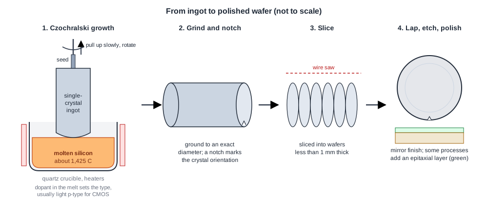
Wafer diameters have grown from 75 mm to the 300 mm used by most modern fabs, with 200 mm still common for mature processes. A 300 mm wafer has 2.25 times the area of a 200 mm wafer, so a tool that handles one wafer at a time processes more than twice as many dies per step, which lowers the cost per die. Each change of size needs a new generation of equipment, so it happens only once every couple of decades.
The Cleanroom and the Lot
A particle the size of a wire's width can short two wires or open one, as Design for Manufacturing and Yield described. Fabs therefore filter their air continuously, keep people in full-body suits, and keep wafers sealed in carriers whenever they are not inside a tool. In a 300 mm fab, the carriers hold up to 25 wafers and are moved between tools by an overhead transport system.
Wafers travel through the fab in lots, usually one carrier each. A lot follows a route, the process recipe: an ordered list of hundreds of steps such as clean, oxidize, coat, expose, develop, etch, implant, anneal, deposit, polish and measure. The fab's scheduling system decides which lot runs next on each tool.
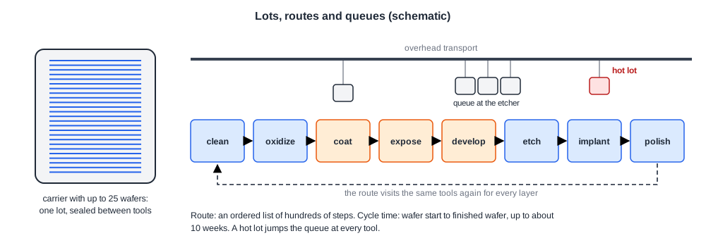
The time from wafer start to finished wafer is the cycle time. Turnaround times of up to 10 weeks are typical, and processes with more layers take longer, because fabs are optimized for throughput, not for the latency of one lot. A customer can pay for a hot lot that jumps the queue at every tool, at the price of disrupting everyone else's schedule.
One Lithography Cycle
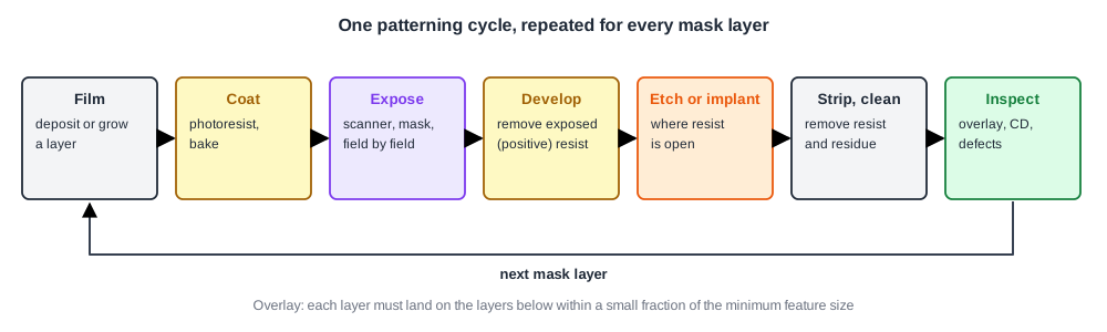
- Film. A layer is grown or deposited: oxide by heating the wafer in oxygen or steam, other films by chemical vapour deposition, metals by sputtering. Some cycles have no new film; they only mask an implant.
- Coat. The wafer is spun with photoresist, a light-sensitive polymer, and baked.
- Expose. The scanner aligns the mask to the patterns already on the wafer, then exposes one field, steps to the next and repeats.
- Develop. For a positive resist, the developer dissolves the exposed areas; for a negative resist, the unexposed ones. Positive resists give higher resolution and are the usual choice.
- Etch or implant. Where the resist is open, a plasma etches the film below, or an ion implanter drives dopant atoms into the silicon. The resist protects everything else.
- Strip and clean. The resist is removed and the wafer cleaned of residue.
- Inspect. Metrology tools measure the critical dimension (the printed width), the overlay (how well this layer lands on the layers below) and the defects. A lot that fails can often be reworked: the resist is stripped and the exposure repeated, before the etch makes it permanent.
Quick Check
Q: The overlay measurement after develop shows that the contact layer is shifted against the poly below. Why is it cheaper to find this before the etch than after?
Show Answer
Before the etch, the pattern exists only in the resist. The resist can be stripped and the layer exposed again at no cost to the wafer. After the etch, the misplaced contact holes are cut into the dielectric and cannot be undone, so the wafers would be scrapped or would produce failing dies.
How Small Can It Print?
The smallest pitch (line plus space) a lens can print is given by the Rayleigh relation:
pitch = k1 x wavelength / NA
NA is the numerical aperture of the lens, a measure of how wide a cone of light it collects. k1 is a process factor that depends on the resist, the illumination and the resolution enhancements described in From GDSII to Masks; values near 0.8 are easy, near 0.5 very hard.
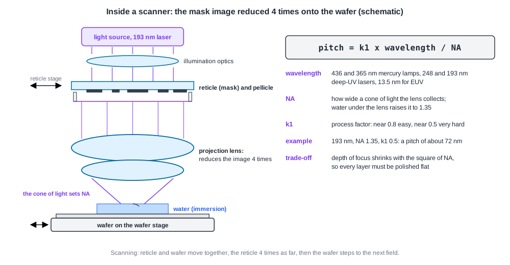
Fabs have reduced the wavelength step by step: mercury lamps at 436 and 365 nm, then deep-UV lasers at 248 nm and 193 nm. Filling the gap between the lens and the wafer with water raises the NA above 1, to 1.35. With 193 nm, NA 1.35 and k1 = 0.5, the best pitch is about 72 nm. Smaller pitches need multi-patterning or extreme ultraviolet light at 13.5 nm, which the most advanced processes use for their critical layers.
Resolution comes with a cost in depth of focus, which shrinks with the square of the NA. A high-NA exposure prints well only on a very flat surface, which is one reason why every layer is polished flat before the next one is patterned, and why metal density rules exist.
Fields and Dies on the Wafer
A modern scanner exposes a field of at most 26 x 33 mm on the wafer. That field limits the size of a single die: a larger chip has to be built from several pieces, as some processors and image sensors are. Within the limit, the reticle holds as many dies as fit, and the scanner steps the field across the wafer.
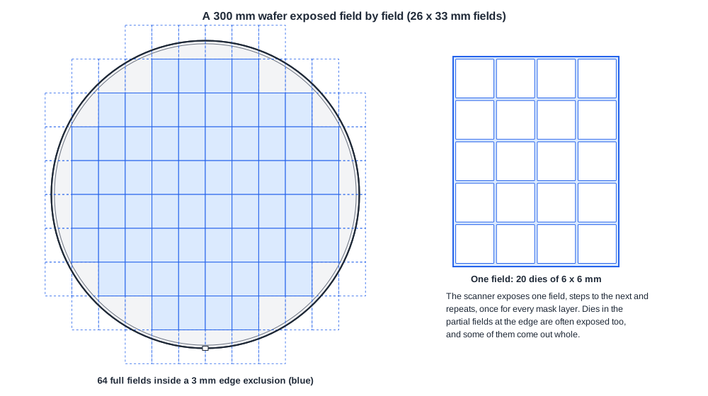
On a 300 mm wafer with a 3 mm edge exclusion, 64 full fields fit on a regular grid. The partial fields at the edge are usually exposed too, because the dies inside them that land completely within the usable area are still good dies. For a 6 x 6 mm die the field holds 20 dies.
Quick Check
Q: Why does the scanner keep exposing the partial fields at the wafer edge, even though most of each field falls off the wafer?
Show Answer
A partial field still contains some complete dies inside the usable area, and those dies are as good as any other. Exposing the edge fields also keeps the pattern, and therefore etch and polish loading, more uniform near the edge.
Running It in ChipVerify Lab
Run Place and Route on the multiplier and read the die size in the report: 175.465 um on each side. With a 0.1 mm scribe lane between dies, a 26 x 33 mm field could hold 94 x 119 = 11,186 copies of it, and 64 full fields would give over 700,000 per wafer. Real chips are much larger, which is why the next articles count dies on the wafer and the share of them that work.
Common Mistakes
Mistake #1: Thinking of lithography as one step
Every mask layer needs its own coat, expose, develop and etch or implant cycle, with overlay to all layers below.
Mistake #2: Forgetting the field limit
A die cannot be larger than the exposure field. Very large designs must be split or stitched.
Mistake #3: Ignoring flatness
High-resolution exposure has a shallow depth of focus. Uneven density makes uneven surfaces and prints badly.
Practice Exercise
Challenge: The Resolution Factor
The sky130 met1 pitch is 0.34 um. A scanner uses 248 nm light with a numerical aperture of 0.75. What k1 would it need to print this pitch, and is that easy or hard? What pitch could a 193 nm immersion scanner with NA 1.35 reach at k1 = 0.5?
Hint
Rearrange the relation: k1 = pitch x NA / wavelength.
Solution
k1 = 0.34 x 0.75 / 0.248 = 1.03, comfortably above the easy region near 0.8. The immersion scanner reaches 0.5 x 193 / 1.35 = 71.5 nm, about 72 nm pitch, nearly five times finer.
Open the ready-made example in the lab, synthesize it and run Place and Route.
Summary
- Wafers are sliced from Czochralski single-crystal ingots and polished flat; 300 mm is the modern standard, 200 mm common for mature processes.
- Wafers move in lots along a route of hundreds of steps; cycle time is weeks to months, and hot lots trade cost for speed.
- Each mask layer goes through coat, expose, develop, etch or implant, strip and inspect, with rework possible before the etch.
- Resolution follows k1 x wavelength / NA; shorter wavelengths, immersion, multi-patterning and EUV push it down.
- A scanner field of 26 x 33 mm limits the die size; 64 full fields fit on a 300 mm wafer with a 3 mm edge exclusion.