
An I/O cell connects the chip's core logic to a pad. It drives outputs strongly enough to charge a board trace, turns noisy external inputs into clean core levels, shifts between the core voltage and the I/O voltage, and protects the thin-oxide core from electrostatic discharge. I/O cells come from the foundry or a library vendor as hard cells, like memories. This article looks inside one, the sky130 general-purpose I/O cell, using its library files: its size, its pins, its supplies, and the options it gives the designer.
8 min read | Intermediate
What You'll Learn
- Describe the parts of an I/O cell: driver, receiver, level shifters and ESD protection
- Read the pins and supplies of the sky130 GPIO cell
- Explain drive modes, slew control and input options
- Describe how an I/O cell's layout connects to the core and to the pad ring
What Is Inside an I/O Cell
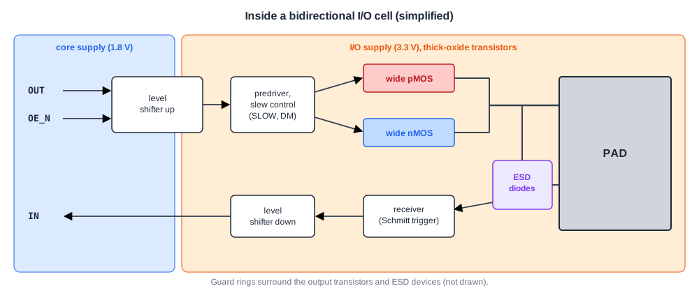
An I/O cell has a standard set of parts, and the sky130 cell has all of them:
- Output driver. Very wide pMOS and nMOS transistors, folded into many legs, sized to charge an external load of typically 2 to 50 pF within the required edge time. A chain of buffers, the predriver, builds up from the small core signal to these large gates.
- Tristate control. An enable turns both output transistors off so the pad can be an input. Many libraries offer only a bidirectional cell, used as an input or an output by tying the enable.
- Input receiver. A buffer, often a Schmitt trigger with hysteresis, that cleans up slow or noisy edges. Optional weak pull-up or pull-down resistors give an unconnected pad a known value.
- Level shifters. The core runs at a lower voltage than the I/O, so signals are shifted up on the way out and down on the way in. The parts that see the I/O voltage use thick-oxide transistors.
- ESD protection. Clamp diodes and resistors between the pad and the supplies, described in ESD Protection for Physical Designers.
The output transistors also need guard rings. Ringing on a bond wire can push the pad above the I/O supply or below ground, forward-biasing the drain junctions and injecting current into the substrate, which can trigger latch-up. The usual practice is to surround output transistors with double guard rings and keeping them well away from internal circuits.
The sky130 GPIO Cell
The sky130 I/O library's general-purpose cell, sky130_fd_io__top_gpiov2, is 80 um wide and 200 um tall according to its LEF, which declares it CLASS PAD. Its pins fall into four groups:
| Group | Pins | Purpose |
|---|---|---|
| Core side | OUT, OE_N, IN | data to the pad, output enable (active low), data from the pad |
| Configuration | DM[2:0], SLOW, VTRIP_SEL, INP_DIS, IB_MODE_SEL, HLD_H_N, ENABLE_H and others | drive mode, slew rate, input threshold, input disable, hold |
| Pad and analog | PAD, AMUXBUS_A, AMUXBUS_B, PAD_A_ESD_0_H and others | the pad itself, analog buses, analog access to the pad |
| Supplies | VDDIO, VDDIO_Q, VDDA, VCCD, VSWITCH, VCCHIB, VSSD, VSSIO, VSSIO_Q, VSSA | I/O, analog and core supplies and grounds |
Pins whose names end in _H work at the I/O supply level, not at the core level. That matters for the designer: a core gate cannot drive ENABLE_H directly, so these controls come from logic in the I/O supply domain or are tied off.
Drive modes
The three DM bits choose how the output drives the pad. The cell's behavioral model in the library shows eight modes:
| DM | Output behavior |
|---|---|
| 000 | off, and the input buffer disabled |
| 001 | output off: input only |
| 010 | strong 0, resistive pull-up for 1 |
| 011 | strong 1, resistive pull-down for 0 |
| 100 | open drain: strong 0, high impedance for 1 |
| 101 | open source: strong 1, high impedance for 0 |
| 110 | strong push-pull |
| 111 | weak pull-up and pull-down |
SLOW selects a slower output edge. A slower edge means less current change per nanosecond, and therefore less supply noise when many outputs switch together, as Power and Ground Pads: How Many and Where calculates. VTRIP_SEL selects the input switching threshold, so the same cell can receive signals of different voltage standards.
Quick Check
Q: A pin must be shared by several chips on a board, any of which may pull it low, with one resistor pulling it high. Which drive mode fits?
Show Answer
Open drain, DM = 100. Each chip can only pull the line low or release it, so two chips can never fight with opposite strong levels. The external resistor provides the high level when every chip releases the line.
The Layout of an I/O Cell
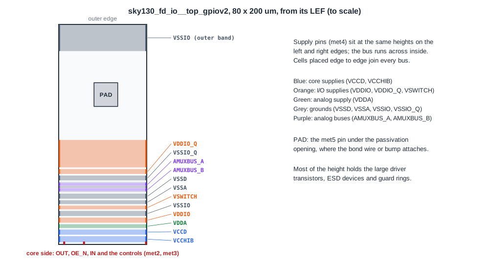
The LEF shows how the cell is built to sit in a ring:
- Core side. The signal pins (OUT, OE_N, IN and the controls) sit at one edge, on met2 and met3, facing the core. The top-level router connects them to the core logic.
- Supply buses. VCCD, VDDA, VDDIO, VSSD, VSSIO and the others appear as met4 pins on both side edges of the cell, at exactly the same heights on the left and the right, and inside the cell each bus runs across between them. Placed edge to edge, neighbouring cells touch pin to pin and join the buses into continuous rings around the die, with no routing. This is called connection by abutment. The buses fill the lowest 95 um of the cell, next to the core side, and VSSIO also has a wide band along the outer edge.
- Pad. The PAD pin is on met5, the top metal, near the outer edge, under the opening in the passivation where the bond wire or bump attaches.
The cell is tall because most of its height holds the large driver transistors, the ESD devices and their guard rings, which cannot shrink with the core logic. An inverter in the core is a few micrometres wide; the cell that drives a signal off the chip is 80 x 200 um.
Other Cells in an I/O Library
A pad ring needs more than signal cells. The sky130 library and its open-source wrappers include:
- Supply pads, 75 um wide, for each supply, with ESD clamps: "high-voltage clamp" versions for the 3.3 V supplies and "low-voltage clamp" versions for the 1.8 V ones.
- A reset input cell with a glitch filter,
top_xres4v2. - Corner cells, 200 x 204 um, that turn the supply buses around the corners of the die.
- Filler slices 1, 5, 10 and 20 um wide that carry the buses between cells, and slices that deliberately connect or disconnect particular buses.
How these are combined into a ring is the subject of Building the Pad Ring.
Quick Check
Q: Why does the GPIO cell have each supply pin twice, on its left and right edges, at exactly the same height?
Show Answer
So that cells placed edge to edge connect their buses automatically. Each cell's right-edge pin touches its neighbour's left-edge pin of the same supply, and the bus inside each cell joins its two pins, forming a ring around the die without any routed wires.
Timing Through an I/O Cell
The I/O cell is part of every chip-level timing path that leaves or enters the die. Its output delay depends strongly on the external load, which the core designer does not control, and its input delay on the edge rate arriving from the board. The I/O library supplies Liberty models for these delays, and the chip's constraints describe the board: set_load on the output ports and set_input_transition on the inputs, as in Modeling the I/O Environment.
A block-level run like the lab's has no I/O cells, so its input and output delays are budgets. At the chip level, the budget must include the I/O cell's delay at the board load, which can be several nanoseconds for a slow, high-voltage output.
Running It in ChipVerify Lab
At the time of writing, the lab's flow has no sky130 I/O cells. The numbers in this article come from the I/O library's LEF, its pin definitions and its behavioral Verilog model. You can still see the scale difference: run Place and Route on the multiplier and compare its die, a fraction of a millimetre on each side, with one 80 x 200 um GPIO cell.
Common Mistakes
Mistake #1: Driving I/O-level control pins from core logic
Pins at the I/O supply level need I/O-level signals. Check every pin's voltage domain in the library documentation.
Mistake #2: Using the fastest edge everywhere
Fast output edges increase supply noise. Use slow mode on every output whose timing allows it.
Mistake #3: Leaving unused pads floating
A floating input can sit between the logic levels and draw current. Use a pull mode or tie the input.
Practice Exercise
Challenge: Configure Three Pins
Choose the sky130 GPIO drive mode for: (a) a push-pull clock output to another chip; (b) an input that must read high when nothing is connected; (c) an interrupt line shared by four chips with an external pull-up.
Hint
Look for strong, weak and high-impedance levels in the drive mode table.
Solution
(a) DM = 110, strong push-pull. (b) A mode with a resistive pull-up and the output not driving low: DM = 010 with OUT = 1 gives a resistive 1 while still letting an external driver pull the pin low, and the input buffer stays enabled. (c) DM = 100, open drain, with OUT = 0 to pull low and OUT = 1 to release.
Summary
- An I/O cell holds an output driver, tristate control, an input receiver, level shifters and ESD protection.
- The sky130 GPIO cell is 80 x 200 um, with core-side pins on met2 and met3, supply buses on met4 with pins at the same heights on both side edges, and the pad on met5.
- Its DM bits select eight drive modes; SLOW reduces edge rates and VTRIP_SEL selects the input threshold.
- Pins ending in _H work at the I/O supply level.
- I/O cell delays depend on the board load and belong in every chip-level timing budget.
