
After the wafers leave the fab, the same handful of steps turn them into products: wafer sort (probing every die on the wafer), sometimes bumping, then thinning, dicing, assembly into packages, final test and shipping. Which company does each step, and where the wafers travel in between, depends on the business model. A company that owns its fabs may never let a wafer leave its own sites; a fabless company may never see its wafers at all; and some fabless companies probe every wafer in their own test floor before any package is made. This article lays out the roles and the common flows, and what physically moves between them.
8 min read | Intermediate
What You'll Learn
- Name the companies involved after tapeout and what each one does
- Trace seven common flows from finished wafer to shipped part
- Explain why and where wafers are tested before packaging
- Describe what ships between companies: wafers, maps, dies and parts
The Steps After Wafer Out
Back-End-of-Line and Wafer Out ended with finished wafers that passed the foundry's wafer acceptance test. From there, the steps are the same in every flow, even if different companies perform them:
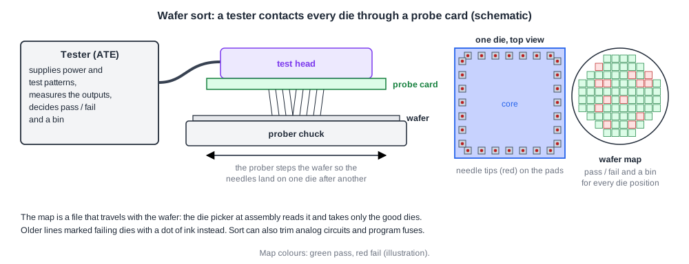
- Wafer sort (also called probe or circuit probe). A tester contacts every die through a probe card and runs a test program on it. The result is a wafer map: pass or fail, often with a bin number, for each die position.
- Bumping, for flip-chip and wafer-level packages: solder bumps or pillars and any redistribution layer are added to the whole wafer.
- Thinning and dicing. The wafer is ground thinner from the back, mounted on tape and cut into dies along the scribe lanes.
- Assembly. Good dies are picked according to the wafer map, attached to a package and connected, as described in Dicing and Packaging.
- Final test, sometimes with burn-in: every packaged part is tested again, and often sorted into speed or power grades.
How these tests are written and run is a subject of its own; here they matter as steps in the flow.
The Players
- IDM (integrated device manufacturer): designs chips and owns the fabs, and usually its own assembly and test sites.
- Fabless company: designs and sells chips, owns no fab.
- Foundry: manufactures wafers for others. A pure-play foundry makes no chips of its own.
- OSAT (outsourced semiconductor assembly and test): bumps, dices, packages and tests for others, and often runs wafer sort too.
- ASIC or design-service vendor: takes a customer's specification, RTL or netlist and delivers finished parts, managing the foundry and OSAT on the customer's behalf.
- Shuttle or MPW organizer: collects many small designs onto one mask set and distributes the results.
Many companies fill more than one role. Some IDMs also sell foundry capacity; some fabless companies own test floors; some foundries offer bumping, advanced packaging and sort.
Seven Common Flows
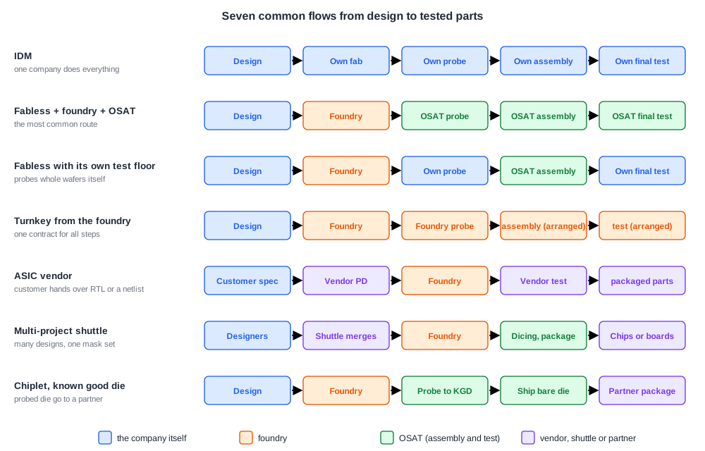
1. IDM: everything in house
The wafers move between the company's own fab, probe floor and assembly and test sites, which may be in different countries. Yield data flows straight back to the process engineers, and the company controls every step and every cost.
2. Fabless, foundry and OSAT
This is the most common flow. The foundry ships the finished wafers, sealed in wafer shippers and usually with the WAT data, directly to the OSAT. The OSAT runs wafer sort with the customer's test program and probe card, dices the wafers, packages the good dies and runs final test. The parts go to the customer's warehouse or straight to its customers. The fabless company may never handle one of its own wafers; what it sees is data: WAT results, wafer maps and test yields.
3. Fabless with its own test floor
Some fabless companies probe their wafers themselves, before anything is packaged. The foundry ships the wafers to the company's probe floor; the company sorts them and then sends the probed wafers and their maps to an OSAT for assembly. Final test may come back in house too. The reasons:
- Fast yield learning. The wafer maps arrive the day the wafers are probed, by the people who designed the chip.
- Control of the test program, which can contain the most sensitive knowledge about the product.
- Expensive testers already owned, for example for RF, analog or high-speed parts.
- First silicon. For a new chip, engineers often probe the first wafers on a probe station in their own lab long before production test exists.
4. Turnkey from the foundry
The foundry, or its partners, provide sort, assembly and test under one contract, and the customer receives finished parts. This suits companies without operations teams, and advanced packages that the foundry builds itself.
5. ASIC vendor
The customer provides a specification, RTL or a netlist. The vendor does the physical design, holds the foundry relationship, develops the test program and delivers tested, packaged parts at a price per part. The customer buys working chips, not wafers.
6. Multi-project shuttle
The organizer merges many designs into one mask set, as described in What Leaves the Design House. After fabrication the wafers go to the organizer, which has them diced and distributes the results. Depending on the programme a designer receives bare dies, packaged parts, or a chip on a board. TinyTapeout, for example, ships a packaged chip on a carrier board that plugs into a demo board, with every project on the chip selectable.
7. Chiplets and known good die
When several dies go into one package, a single bad die spoils the whole, expensive assembly. The dies are therefore tested at wafer level more thoroughly, often to the level of a final test, and shipped as known good die (KGD): bare dies on tape or in trays, to the partner who assembles the multi-die package.
Quick Check
Q: In flow 2, which company has the wafers physically in its hands after they leave the foundry, and what does the fabless company receive instead?
Show Answer
The OSAT. The foundry ships the wafers directly to it for sort, dicing, assembly and final test. The fabless company receives data, such as WAT results, wafer maps and test yields, and finally the tested parts or a delivery to its customers.
Why Test Before Packaging?
In every flow except some very cheap parts, dies are tested on the wafer before they are packaged:
- A package costs money. Packaging a die that would fail wastes the package, the assembly time and the final test time.
- The wafer map is a yield picture. Failures clustered at the edge, in a ring, or along one exposure field point to a process cause; scattered failures point to random defects. That picture is lost once dies are separated.
- Some tests are easier on the wafer. Trimming analog circuits, programming fuses and measuring leakage are often done at sort.
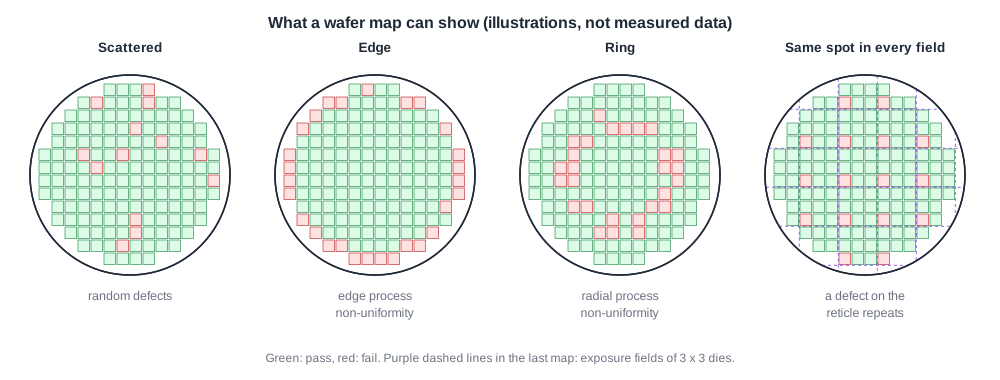
Older lines marked failing dies with a dot of ink; today the wafer map travels as a file with the wafer, and the die-picking machine at assembly reads it.
What Ships Between Companies
| Item | From, to | Form |
|---|---|---|
| Finished wafers | foundry to OSAT, test floor or organizer | sealed wafer shippers, with WAT data |
| Wafer maps | prober to assembly and customer | files with the pass, fail and bin of each die |
| Bare dies | OSAT or organizer to partner or designer | tape frames, trays or waffle packs |
| Packaged parts | OSAT to customer or distributor | trays or tape and reel |
| Test programs and probe cards | company to OSAT or test floor | software and hardware owned by the chip company |
Who pays for bad dies follows from the contract. A fabless company usually buys wafers and owns the yield risk; an ASIC vendor sells good parts and owns it; a KGD supplier guarantees each die it ships.
Quick Check
Q: Why does a chiplet flow test dies more thoroughly at wafer level than a flow that packages each die on its own?
Show Answer
In a single-die package, a bad die that slips through sort is caught at final test and only one cheap package is lost. In a multi-die package, one bad die makes the whole assembly, with its other good dies and its expensive substrate, a failure. Testing harder at wafer level is cheaper than losing those assemblies.
Common Mistakes
Mistake #1: Assuming the foundry tests your chip
The foundry guarantees its process through WAT. Testing the design, at sort and final test, is the chip company's job unless a contract says otherwise.
Mistake #2: Forgetting the test program and probe card in the schedule
Sort cannot start without them, and both take weeks to make. They are needed when the first wafers arrive, not after.
Mistake #3: Throwing away the wafer map
The pattern of failures across the wafer is the best clue to their cause. Keep the maps with the lot data.
Practice Exercise
Challenge: Choose the Flow
Match each company to the flow it most likely uses: (a) a university group with one small test chip, (b) a start-up making a mixed-signal sensor that must be trimmed at wafer level with its own specialised tester, (c) a large company with its own fabs, (d) a systems company that wants custom chips but has no chip design team.
Hint
Ask who owns the fab, who owns the tester and who does the physical design.
Solution
(a) A multi-project shuttle, flow 6. (b) Fabless with its own test floor, flow 3, sorting and trimming the wafers before sending them to an OSAT. (c) IDM, flow 1. (d) An ASIC vendor, flow 5, which does the physical design and delivers tested parts.
Summary
- After wafer out come wafer sort, bumping where needed, thinning and dicing, assembly and final test.
- IDMs keep every step in house; fabless companies split the work between a foundry and an OSAT, and some sort wafers on their own test floors.
- Turnkey foundries and ASIC vendors deliver finished parts; shuttles return bare dies, packaged chips or boards.
- Dies are tested on the wafer to avoid packaging bad dies and to keep the yield picture of the wafer map.
- Wafers, wafer maps, bare dies and packaged parts move between companies, and the contract decides who carries the yield risk.
