
The back-end of line (BEOL) builds the wiring above the transistors: layer after layer of insulating dielectric, vias and metal, each polished flat before the next, and finally a protective passivation with openings over the pads. When the last layer is done, the foundry measures test structures in the scribe lanes to confirm that the wafers came out within the process limits, and ships them. This article follows the sky130 back-end stack with its real heights, compares two ways of making metal wires, and explains how wafer acceptance data connects to the process corners used in timing analysis.
7 min read | Intermediate
What You'll Learn
- Describe the back-end layer sequence and the role of polishing
- Compare subtractive aluminium and damascene copper wiring
- Explain scribe-line test structures and wafer acceptance testing
- Relate wafer acceptance data to the process corners of the libraries
The sky130 Stack
The Metal Stack introduced the sky130 routing layers from the technology LEF. The process stack in the sky130 PDK documentation adds their heights above the silicon. Drawn to scale, with the number of shapes each layer carries in the routed multiplier:
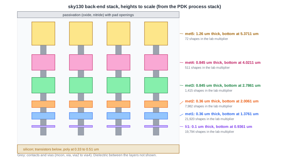
The lower layers are thin and closely spaced for dense local wiring: li1 is 0.1 um thick, met1 and met2 0.36 um. met3 and met4 are 0.845 um, and met5 is 1.26 um, thick enough for low-resistance power distribution, which is why the lab's power grid uses its straps on met4 and met5. The wiring follows the same pattern: the multiplier has 21,920 met1 shapes but only 72 on met5.
The stack figure also names the dielectrics between the layers, with dielectric constants from 3.5 to 4.5 for the inter-level oxides and 7.3 to 7.5 for nitride layers, and a polyimide coating on top. These values are what the extraction rules use to compute the capacitances in Parasitics After Routing.
One Metal Level
Each level repeats the same sequence:
- Deposit the dielectric over the level below and polish it flat.
- Pattern and etch the via holes, and fill them, often with tungsten plugs.
- Form the metal wires of the new level.
- Deposit the next dielectric and polish again.
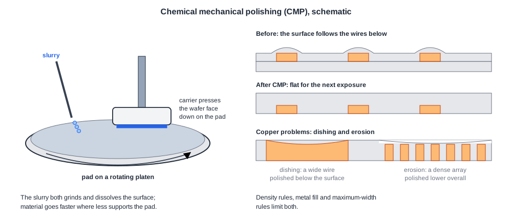
The polishing step is chemical mechanical polishing (CMP): the wafer is pressed against a rotating pad with a slurry that both grinds and dissolves the surface. CMP removes material faster where there is less to support the pad, so areas of very low or very high metal density end up thinner or thicker than the rest. That is the reason for the density rules and metal fill of Filler Cells, Metal Fill and Density Rules: they keep the surface flat enough for the next exposure, whose depth of focus is small.
Aluminium or Copper
There are two ways to form the wires, and they differ in which material is etched:
- Subtractive aluminium. Aluminium is sputtered over the whole wafer, patterned with resist and etched away where no wire is wanted; then the dielectric fills the gaps. This was the standard for decades and is still used in mature processes.
- Damascene copper. Copper conducts better but is hard to etch and poisons transistors if it diffuses into the silicon. So the process works the other way round: trenches and via holes are etched into the dielectric, lined with a thin conductive barrier such as tantalum nitride, filled with electroplated copper, and the excess copper is polished off. In dual damascene the via and the wire above it are filled in one step. The name comes from the inlaid metalwork of medieval Damascus.
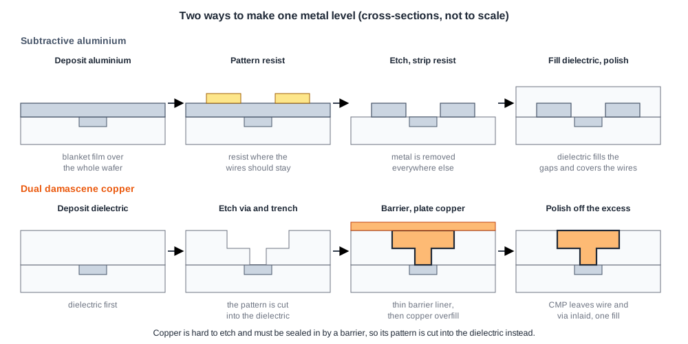
Most modern logic processes use copper with low-k dielectrics; the top layer, used for the pads, is often aluminium. For a physical designer the difference shows up in the rules: damascene layers have density and width-dependent rules tied to polishing and dishing, and copper's barrier liner adds resistance that becomes significant in very narrow wires.
Quick Check
Q: In a copper damascene process, a very wide copper wire comes out thinner in the middle than at its edges. Which process step causes this, and what layout rule addresses it?
Show Answer
CMP. The soft copper in a wide trench is polished down below the surrounding dielectric, an effect called dishing. Maximum width rules, slotting of wide wires and density rules keep the copper areas small and even enough to avoid it.
Passivation and Pads
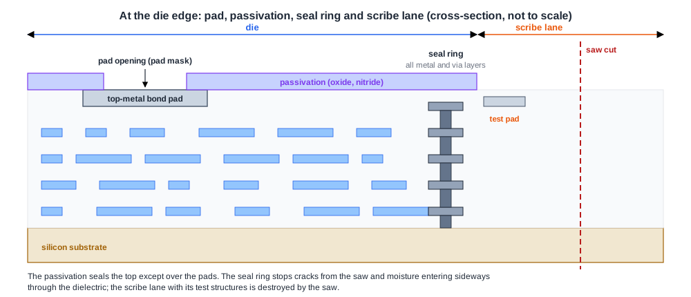
Above the top metal the wafer is sealed with passivation, layers of oxide and nitride that keep out moisture and ions and protect against scratches; some processes add a polyimide coat for packaging stress. The pad mask (PDM in the sky130 list) opens the passivation over the bond pads, the only places where the top metal stays exposed. The seal ring around each die, built from all metal and via layers and joined to the passivation (sky130 has a Nitride Seal Mask, NSM), stops cracks and moisture from entering at the sawn edge later.
Wafer Out: Test Structures in the Scribe
When the last layer is done, the foundry has to show that the wafers were made correctly before it ships them. It does not test the customer's circuits for this; it measures its own test structures, placed in the scribe lanes between the dies, where they cost no die area and are destroyed by the saw later.
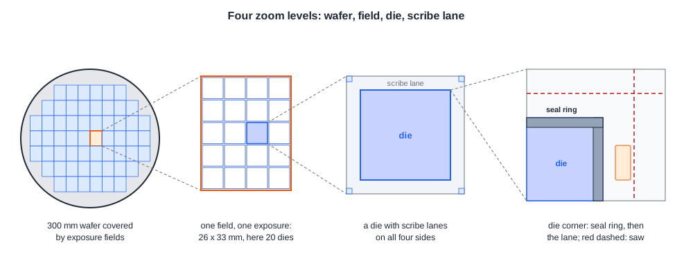
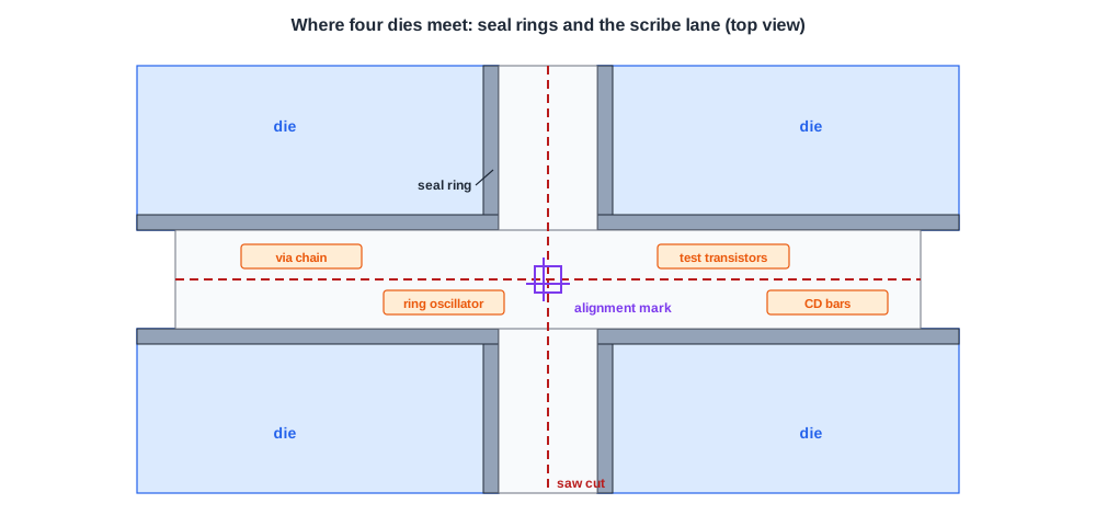
Typical structures:
- Test transistors of every type, for threshold voltage, drive current and leakage.
- Chains of contacts and vias, thousands in series, for contact resistance and opens.
- Sheet resistance structures for each conducting layer.
- Ring oscillators, whose frequency summarizes gate delay in one number.
- Critical dimension and vernier structures for printed widths and layer-to-layer alignment.
The sky130 layer documentation shows how they get there: a marker layer records the location of "e-test modules" within the frame, used by the frame builder to place them in the scribe lane.
Wafer Acceptance Test and Process Corners
The foundry probes these structures on several sites of each wafer. This is called the wafer acceptance test (WAT), or process control monitoring (PCM). Every parameter has a specification window; wafers inside it are shipped, usually with the WAT data, and wafers outside it are held for review or scrapped.
WAT is not a test of the design. A wafer can pass WAT and still have dies that fail, because of a random defect or a design error; finding those is the job of wafer sort, which comes later and is described in Who Does What After Tapeout.
WAT data is also where the process corners come from. Collected over thousands of wafers, it shows how far the transistor parameters spread. The foundry derives the slow and fast corners of its device models from that spread, and the library teams characterize the standard cells at those corners: sky130's ss, tt and ff libraries. When Post-Route STA checks setup at the slow corner and hold at the fast one, it is checking the design against the range that WAT promises the wafers will stay in.
Quick Check
Q: All wafers of a lot pass the wafer acceptance test, yet 20 % of the dies fail at wafer sort. Is this a contradiction?
Show Answer
No. WAT measures the foundry's scribe-line structures on a few sites per wafer and shows that the process parameters are within specification. It says nothing about random defects inside individual dies or about the design itself, which wafer sort tests die by die.
Running It in ChipVerify Lab
Run Place and Route on the multiplier and look at the density section of the report: it shows how evenly each metal layer is filled, the property that CMP depends on. With PRO, the metal fill option adds fill shapes into the GDSII, and the density report shows the layers rising towards the window minimum. The multi-corner option runs timing at the slow and fast corners derived from the process spread described above.
Common Mistakes
Mistake #1: Treating density rules as cosmetic
They exist because CMP thins sparse and dense areas differently, which changes resistance and spoils the flatness the next layer needs.
Mistake #2: Confusing WAT with testing the chip
WAT checks the process on the foundry's test structures. The design is tested at wafer sort and final test.
Mistake #3: Putting design structures in the scribe
Anything in the scribe lane is destroyed by the saw. Test structures you need after dicing belong inside the die.
Practice Exercise
Challenge: Heights in the Stack
Using the sky130 heights above (bottom of each layer and its thickness), how much vertical space separates the top of met1 from the bottom of met2? And the top of met4 from the bottom of met5? Why might a via from met4 to met5 have more resistance than one from met1 to met2?
Hint
Top of a layer = bottom + thickness.
Solution
met1 top = 1.3761 + 0.36 = 1.7361 um, so the gap to met2 at 2.0061 um is 0.27 um. met4 top = 4.0211 + 0.845 = 4.8661 um, so the gap to met5 at 5.3711 um is 0.505 um. The upper via is almost twice as tall, and a taller cut of similar cross-section has more resistance; in practice upper vias are also larger, which partly compensates.
Open the ready-made example in the lab, synthesize it and run Place and Route.
Summary
- The back end repeats dielectric, via and metal steps for every level, each polished flat by CMP.
- In sky130, li1 is 0.1 um thick, met1 and met2 0.36 um, met3 and met4 0.845 um and met5 1.26 um.
- Aluminium wires are etched; copper wires are inlaid into etched dielectric by the damascene process.
- Passivation seals the wafer; pad openings and the seal ring complete each die.
- Scribe-line test structures are measured in the wafer acceptance test, which qualifies wafers for shipment, not individual dies.
- The spread of WAT data defines the process corners used for library characterization and timing sign-off.