
The cell LEF describes every standard cell as an abstract: its size, its pins and the metal it uses inside, without a single transistor. That is all place and route needs to know about a cell. The placer needs the size, the router needs to know where the pins are and which areas inside the cell it must avoid. This article compares the full layout of a sky130 inverter with its LEF abstract and reads the parts of a cell LEF.
7 min read | Beginner to Intermediate
What You'll Learn
- Explain the difference between a cell's full layout and its LEF abstract
- Read MACRO, CLASS, SIZE, SYMMETRY and SITE statements
- Read pin definitions: direction, use, shape and port geometry
- Explain obstructions and the antenna data on pins
Full Layout and Abstract
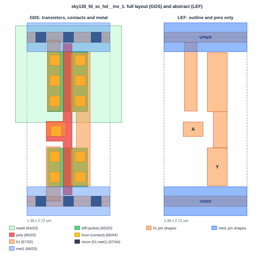
On the left is the real layout of sky130_fd_sc_hd__inv_1 from the library GDS: the n-well (light green), the active areas (green), the poly gate (red) that forms one PMOS transistor at the top and one NMOS transistor at the bottom, the contacts (yellow), the li1 interconnect (orange) and the met1 rails (blue). On the right is its LEF: just the outline, the input pin A and the output pin Y on li1, and the VPWR and VGND rails on met1. Everything else is hidden. Abstracts keep the tool fast and protect the cell design, and the full layouts are merged back only when the GDSII is written.
The MACRO Header
MACRO sky130_fd_sc_hd__inv_1
  CLASS CORE ;
  SOURCE USER ;
  ORIGIN  0.000000  0.000000 ;
  SIZE  1.380000 BY  2.720000 ;
  SYMMETRY X Y R90 ;
  SITE unithd ;
- CLASS: what kind of cell this is. In the sky130 hd LEF, 422 cells are
CORE, the 11 cells that contain well taps (the tap cells and some level shifters) areCORE WELLTAP, and the 4 fillers areCORE SPACER. Large blocks such as memories areBLOCK, I/O cellsPAD. Tools use the class to decide what may go where. - SIZE: 1.38 x 2.72 um, three sites wide.
- SYMMETRY: the cell may be mirrored in X and Y, which is what lets it sit in flipped rows.
- SITE: it fits the
unithdsite of the technology LEF.
Pins
  PIN A
    ANTENNAGATEAREA  0.247500 ;
    DIRECTION INPUT ;
    USE SIGNAL ;
    PORT
      LAYER li1 ;
        RECT 0.320000 1.075000 0.650000 1.315000 ;
    END
  END A
  PIN VGND
    DIRECTION INOUT ;
    SHAPE ABUTMENT ;
    USE GROUND ;
    PORT
      LAYER met1 ;
        RECT 0.000000 -0.240000 1.380000 0.240000 ;
    END
  END VGND
Each pin has a direction (INPUT, OUTPUT, INOUT), a use (SIGNAL, CLOCK, POWER, GROUND) and one or more ports, each a set of rectangles on a layer. The router must land a via on one of these rectangles. Pin A is a small rectangle on li1, so the router reaches it with an mcon via from met1.
The VGND rectangle runs the full width of the cell and extends 0.24 um below it, half of a 0.48 um rail. SHAPE ABUTMENT says that this shape is meant to join the same shape of the neighbouring cell: placed side by side, cells form continuous rails, and a flipped row above shares half of the rail.
ANTENNAGATEAREA on an input is the area of transistor gate connected to the pin, 0.2475 um2 for this inverter. Outputs carry ANTENNADIFFAREA, the diffusion that can drain charge. The router's antenna check uses both.
Quick Check
Q: The flip-flop dfxtp_1 has a pin with USE CLOCK. Which pin, and which tool step cares?
Show Answer
Pin CLK. Clock tree synthesis treats clock pins as the sinks of the clock tree, and some tools route clock nets with special rules. In the sky130 hd LEF, 69 pins are marked as clock pins.
Obstructions
A cell uses metal internally that is not part of any pin. The OBS section lists it, so the router keeps its own wires away. The inverter's OBS section is empty, but the flip-flop has many li1 obstructions:
  OBS
    LAYER li1 ;
      RECT 0.175000 0.345000 0.345000 0.635000 ;
      RECT 0.175000 0.635000 0.840000 0.805000 ;
      ...
If an obstruction were missing, the router could draw a wire across the cell's internal wiring and short it. Missing obstructions are a classic cause of LVS shorts after routing.
Quick Check
Q: The LEF of the inverter shows no transistors and no contacts. How does the final GDSII get them?
Show Answer
When the layout is streamed out, the tool places the full GDS layout of each cell, taken from the library GDS, at the position and orientation given in the DEF. The LEF abstract is only used during place and route.
Running It in ChipVerify Lab
Run Place and Route on the counter and zoom in on a cell in the layout viewer. The wires reach the cells' pins on li1 through vias, and stay off the cells' internal metal.
Common Mistakes
Mistake #1: Trusting an abstract that does not match the layout
If a pin in the LEF is not where the GDS has it, or an obstruction is missing, the routed design fails LVS. Abstracts generated from the GDS by a tool are safer than hand-written ones.
Mistake #2: Ignoring the CLASS of a cell
Tools pick cells by class. An antenna diode must be marked CORE ANTENNACELL for the router to insert it automatically; in the sky130 hd LEF used by the lab, diode_2 is plain CORE, and OpenROAD warns that it found no antenna cell.
Practice Exercise
Challenge: Pins of a Flip-Flop
From the LEF data in this article: the input D of dfxtp_1 has an antenna gate area of 0.126 um2 and CLK has 0.159 um2. The inverter's input has 0.2475 um2. Which input presents the largest gate to the net that drives it, and what does that suggest about the inverter?
Hint
The gate area is roughly proportional to the input capacitance.
Solution
The inverter's input A, at 0.2475 um2, about twice the D input. An inverter input drives the gates of both its PMOS and NMOS transistors directly, while the flip-flop's D input only drives a small input stage. Larger gate area means more input capacitance, which the Liberty file confirms.
Open the ready-made example in the lab, synthesize it and run Place and Route.
Summary
- A cell LEF is an abstract: size, pins and obstructions, without transistors.
- The header gives the class (CORE, CORE WELLTAP, CORE SPACER, BLOCK, PAD), size, symmetry and site.
- Pins have a direction, a use and port rectangles; power rails use
SHAPE ABUTMENTto join neighbours. - Obstructions keep the router away from internal metal; antenna areas feed the antenna check.
