
Hierarchical physical design splits a large chip into blocks that are placed and routed separately and then assembled at the top level, where each finished block appears as a macro. It keeps run times manageable, lets teams work in parallel and allows a block to be reused. The price is that every block needs an exact contract with the top level: its outline and pins, its timing at the boundary, its power connections and its share of the timing budget. This article hardens the routed 16x16 multiplier into such a block and reads the two views the top level uses: the LEF abstract and the Liberty timing model.
7 min read | Intermediate
What You'll Learn
- Weigh flat against hierarchical implementation, and hard against soft macros
- Generate a LEF abstract and a timing model from a routed block
- Read the pins, obstructions and power pins of a block abstract
- Explain timing budgets and how a timing model represents a block
Flat or Hierarchical
A flat flow places and routes the whole design at once. The tools see everything, so they can optimize across any boundary, but run time and memory grow with the design, and every change means a new run of the whole chip. A hierarchical flow implements each block on its own and assembles the results:
- Smaller runs. Each block run is a fraction of the chip, and blocks run in parallel.
- Stable results. A finished block does not change when another block is reworked.
- Reuse. A hardened block can be instantiated many times, like a processor core in a multi-core chip.
- Boundaries are fixed. Paths that cross a block boundary are optimized in two parts, against a budget, and the pin positions constrain both sides.
Hard Macros, Soft Macros and Firm IP
"Macro" and "IP" are used loosely in industry, and the same words can mean slightly different things in different companies and tools. Two meanings are common, and it helps to keep them apart.
The first is about what form a reusable block is delivered in, usually when it comes from an IP vendor, a foundry or another team:
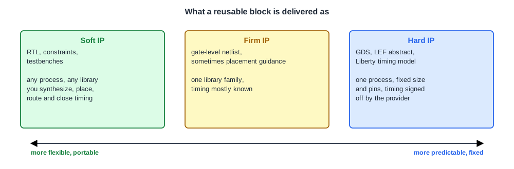
| Soft macro (soft IP) | Firm IP | Hard macro (hard IP) | |
|---|---|---|---|
| Delivered as | synthesizable RTL, constraints, testbenches | gate-level netlist, sometimes with a floorplan or placement guidance | finished layout: GDS, LEF abstract, Liberty timing model, often a behavioral model |
| Tied to a process | no: synthesized with your library | to a library family | yes: one process, one metal stack |
| Can be changed | parameters, configuration, even the RTL | little | nothing: placed as a black box |
| Timing and area | depend on your synthesis and place and route | mostly known | known and characterized |
| Who closes timing inside | you | shared | the provider |
| Typical examples | processor cores, bus interconnect, peripherals, controllers | blocks a vendor wants to protect or pre-optimize | SRAMs and register files, PLLs, data converters, I/O cells, high-speed SerDes and memory PHYs |
Anything analog, or with transistor-level circuits such as memory bit cells, must be hard: there is no RTL that a standard cell flow could turn into it. The OpenRAM SRAM of Macro Placement: Halos and Channels is a hard macro in exactly this sense. Digital functions are usually licensed soft, because the buyer can retarget them to any process and library and fold them into their own flow. The cost of that freedom is that the buyer owns the timing closure, while a hard macro arrives with its timing already signed off.
The second meaning is about how a block is implemented inside a hierarchical chip:
- Hard block, or hard macro. Implemented on its own, as the multiplier is below, and placed at the top level as a fixed macro through its abstract and timing model. Its insides never change during top-level work.
- Soft block, or soft macro. Kept as a logical group of cells that is placed together, inside a region or fence at the top level, but placed and routed in the same run as the rest of the chip. The tool can still optimize across its boundary, and its shape can still change.
Teams often start a block soft and harden it once its size, pins and timing are stable. The same piece of RTL can therefore be a soft IP that a team bought, then a soft block in early floorplans, then a hard macro at tapeout. The multiplier of this tutorial follows that path: it starts as RTL, and below it becomes a hard macro with its own LEF and Liberty views.
Hardening the Multiplier
After routing and extraction, two commands write the views the top level needs:
set_input_delay 2.0 -clock clk [get_ports {a* b*}]
set_output_delay 3.0 -clock clk [get_ports {p*}]
read_spef layout.spef
write_abstract_lef mult16_abstract.lef
write_timing_model -library_name mult16_lib -cell_name mult16 mult16_model.lib
The input and output delays are the block's timing budget: they say how much of the clock period the logic outside the block uses on each side. The abstract is 3,067 lines (118 kB) and the timing model 1,599 lines (52 kB), against 1.31 MB for the block's full DEF.
The LEF Abstract
The abstract describes the block the way a cell LEF describes a standard cell, as covered in Cell LEF, only larger:
MACRO mult16
  FOREIGN mult16 0 0 ;
  CLASS BLOCK ;
  SIZE 175.465 BY 175.465 ;
  ...
  PIN a\[0\]
    DIRECTION INPUT ;
    USE SIGNAL ;
    PORT
      LAYER met2 ;
        RECT  58.12 0 58.26 0.485 ;
- Outline.
CLASS BLOCKand the size, 175.465 um square: the area the top level must reserve. - Signal pins. 65 pins, each a small met2 rectangle on the bottom edge, where the block's pin placer put them. The top-level router must reach exactly these shapes.
- Power pins.
VDDandVSSas pins withUSE POWERandUSE GROUND, made of the block's met4 and met5 straps. - Obstructions. Rectangles on each layer that the top level must not route through: 1 on li1, 25 on met1, 78 on met2, 17 on met3, 13 on met4 and 1 on met5. They merge the block's wiring into coarse areas, keeping only the gaps where top-level routes may pass.
The power pins deserve a note. The block's own database has no power terminals, which is why its power grid check needed -dont_require_terminals in Antenna, ERC and Density Checks. The abstract writer exports the shapes of the supply nets on the top layers as pins. The top-level grid must connect to those straps, so the block's grid and the top-level grid have to be planned together: layers, directions and pitches that line up.
Quick Check
Q: Why does the abstract replace thousands of block wires with a few dozen obstruction rectangles per layer?
Show Answer
The top-level router only needs to know where it may not route, not the block's individual wires. Coarse obstructions keep the abstract small and the top-level run fast. The cost is that the top level cannot use small gaps between the block's wires, only the free areas the obstructions leave open.
The Timing Model
The timing model is a Liberty cell for the whole block. Instead of the block's 1,300 internal nets, it holds only the timing at the pins:
cell (mult16)  area : 9999.574
pin("a\[0\]")  capacitance : 0.0047;
  timing_type : hold_rising;   related_pin : "clk";  values("0.30590")
  timing_type : setup_rising;  related_pin : "clk";  values("-0.28426")
pin("p\[0\]")  timing_type : rising_edge;  related_pin : "clk";
  cell_rise  load 0.0005 ... 0.162 pF:  0.608 ... 1.648 ns
pin("clk")  min_clock_tree_path  0.318 ns
- Inputs become setup and hold constraints relative to the clock pin, as for a flip-flop. Input
a[0]goes straight to an operand register, and the clock reaches that register 0.32 ns after the clock pin, so the setup requirement at the pin is negative (-0.28 ns) and the hold requirement positive (+0.31 ns). - Outputs become clock-to-output delays that depend on the load the top level puts on the pin: from 0.61 ns with almost no load to 1.65 ns with 162 fF.
- The clock pin carries the block's clock tree latency, 0.32 to 0.34 ns, so the top level can balance it against the other clock sinks.
All 32 inputs have a setup and a hold arc and all 32 outputs a clock-to-output arc. Paths that stay inside the block, such as the 32-stage path through the multiplier array, are not in the model at all: they were signed off in the block run and the top level can neither see nor change them.
Quick Check
Q: The model gives input a[0] a setup time of -0.28 ns. How can a setup time be negative?
Show Answer
The requirement is measured at the block's pins. Inside the block, the clock travels through 0.32 ns of clock tree before it reaches the register that a[0] feeds, while the data path from the pin to the register is short. The data can therefore arrive slightly after the clock edge at the clock pin and still meet the register's own setup time.
Budgets
A path from a register in one block to a register in another runs through two blocks and the top-level wires between them. Each block is implemented against its share: here the multiplier assumed its inputs arrive 2 ns after the clock and its outputs must be ready 3 ns before the next edge. If the top level and the neighbouring blocks cannot meet those numbers, the budget is renegotiated and a block is reworked. Good partitioning puts registers at block boundaries, so that the cross-boundary paths are short and the budgets easy to meet.
Running It in ChipVerify Lab
At the time of writing the lab runs one flat Place and Route job per design, with no hierarchical flow. With PRO, the write_abstract_lef and write_timing_model lines can be added at the end of a custom script to produce the two views of a block shown above; the flow already sets input and output delays, and the PRO power pins option gives the block the power pins its abstract needs.
Common Mistakes
Mistake #1: Hardening a block without I/O budgets
Without input and output delays, the block's boundary paths are unconstrained and the timing model describes a block that was never checked at its pins.
Mistake #2: Planning the block grid on its own
The top-level power grid connects to the block's power pins. Layers, directions and pitches must be agreed between block and top.
Mistake #3: Cutting through critical paths
A block boundary in the middle of a long combinational path splits it into two budgeted halves that are hard to close. Place boundaries at registers.
Mistake #4: Assuming "macro" means the same thing to everyone
A vendor's "soft macro" is RTL; a floorplanner's "soft macro" is a placement group. Ask what is delivered and how it will be implemented.
Practice Exercise
Challenge: Using the Model
At the top level, the multiplier's output p[0] drives a wire and a register input with 24 fF in total. The model gives a clock-to-output delay of 0.761 ns at 23.6 fF. The receiving register in another block has a setup time of 0.13 ns, and the clock reaches it 0.40 ns after the clock reaches the multiplier's clock pin. With a 10 ns clock and 1.2 ns of top-level wire delay, what is the slack?
Hint
Arrival = clock-to-output + wire delay. Required = period + capture clock arrival - setup.
Solution
Arrival = 0.761 + 1.2 = 1.96 ns. Required = 10 + 0.40 - 0.13 = 10.27 ns. Slack = 10.27 - 1.96 = 8.31 ns. The model's clock-to-output delay already includes the block's internal clock tree and output path, so the top level only adds what is outside the block.
Open the ready-made example in the lab, synthesize it and run Place and Route.
Summary
- Hierarchical design implements blocks separately and assembles them as macros, trading cross-boundary optimization for smaller, parallel, stable runs.
- Soft IP is delivered as RTL and closed by the user; hard IP as a finished, characterized layout for one process; a soft block is placed as a group in the top-level run, a hard block as a fixed macro.
- The multiplier was hardened into a 175 um block with
write_abstract_lefandwrite_timing_model. - Its abstract has 65 met2 signal pins, VDD and VSS pins on the met4/met5 straps, and coarse obstructions per layer.
- Its timing model turns inputs into setup and hold arcs and outputs into load-dependent clock-to-output delays; internal paths are not visible.