
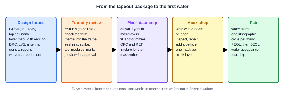
At tapeout the design house sends the foundry a tapeout package: the final GDSII (or OASIS) file of the chip, the facts the foundry needs to manufacture it, and the evidence that it passed sign-off. The foundry checks the package, places the chip into a frame with scribe lanes and test structures, and only then starts making masks. This article walks through what is in that package, what the foundry does with it before the first mask is written, and how a chip can either own a whole mask set or share one with other designs on a multi-project wafer.
7 min read | Intermediate
What You'll Learn
- List the files and facts that make up a tapeout package
- Describe the foundry's tapeout review and frame merge
- Compare a dedicated mask set with a multi-project wafer
- Check a lab GDSII for what a chip still needs before tapeout
The Tapeout Package
GDSII Out and Tapeout showed how the layout becomes a GDSII file. That file is the heart of the package, but the foundry needs more than shapes to build a chip:
- The layout file. GDSII or its more compact successor OASIS, with the name of the top cell. The foundry builds exactly what is in this cell and everything it references.
- The process and its options. The process name and the PDK version the design was checked against, the metal stack option, and any optional devices the design uses, such as thick-oxide transistors, high-resistance poly or a capacitor layer. Each option adds masks and process steps, so it must be ordered explicitly.
- The layer map. Which GDS layer and datatype numbers carry which drawn layer. In sky130, for example, met1 is 68/20 and its pins are 68/16.
- Sign-off results. The DRC, LVS, antenna, density and ERC reports from the foundry's own rule decks, with every remaining violation listed and explained as a waiver.
- Die facts. The die size, the seal ring the design includes or expects, the scribe lane width, the chip and mask revision text, and the pad or bump locations for packaging.
- Third-party IP. Any foundry or vendor IP inside the design, such as I/O pads, memories or analog blocks, identified so the foundry can confirm the approved versions were used.
Most foundries collect these facts on a tapeout form. A wrong entry on the form, such as a missing option, can produce a chip that matches its GDSII perfectly and still does not work, because a layer the design relies on was never made.
The Foundry's Tapeout Review
The foundry does not take the design house's word for it. Before any mask is written, its tapeout team:
- Re-runs sign-off DRC with its own production rule deck, which may be newer or stricter than the deck in the PDK the design team used. New violations go back to the customer.
- Checks the form against the file. If the GDSII contains shapes on an optional layer that was not ordered, or the die size on the form does not match the file, the tapeout stops.
- Merges the chip into the frame. The frame is the layout of everything around the dies on the reticle: scribe lanes, alignment marks, and process test structures. The sky130 documentation names marker layers used by the foundry's frame builder, for the die position, for the frame boundary, and for the "e-test modules" placed in the scribe lane.
- Returns a view of the result for the customer to approve: the die placed in the frame, with the scribe and test modules around it. Only after approval does mask data preparation start.
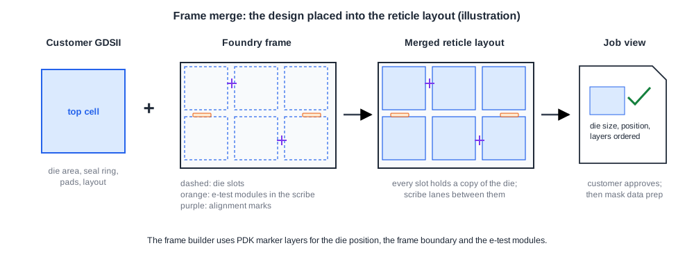
The review usually takes days. A rejected tapeout costs a schedule slip, not money spent on masks, which is why both sides prefer to find problems here.
Quick Check
Q: The design passed DRC with the rule deck shipped in the PDK, but the foundry's tapeout review reports new violations. How can that happen without anything being wrong in the design flow?
Show Answer
The foundry runs its own production deck, which can be newer than the PDK release the team used, or include checks that are not in the public deck. A PDK version mismatch is the most common cause, which is why the PDK version belongs in the tapeout package and why teams re-check against the latest deck before tapeout.
A Lab Block Is Not Yet a Tapeout
The routed 16x16 multiplier from the lab is a clean block: 0 violations in 203 categories of the sky130 KLayout DRC deck, and an LVS match with 1,286 devices and 1,318 nets on both sides. Its GDSII is 1.61 MB, holds 65 cell definitions and has shapes on 34 layer and datatype pairs, from the n-well (64/20) to met5 (72/20), plus pin, label and boundary layers.
Measured against the package above, it still lacks almost everything that makes a chip:
- No pads. Its 65 pins are small met2 shapes (69/16) on the block edge, sized for a router, not for a bond wire or a probe needle.
- No seal ring and no scribe lane. The die boundary is the block's own 175.465 um outline.
- No chip-level fill. Density rules apply to the whole die, as Filler Cells, Metal Fill and Density Rules explained.
- No chip ID or revision text, the small layout text that identifies a die under a microscope after packaging is opened.
A block like this reaches silicon as part of a larger chip, or through a programme that provides the rest, as the next section describes.
Dedicated Masks or a Shared Wafer
A mask set is a large fixed cost. A 65 nm mask set cost about $3 million, and the cost roughly doubles with each newer node. There are two ways to pay it:
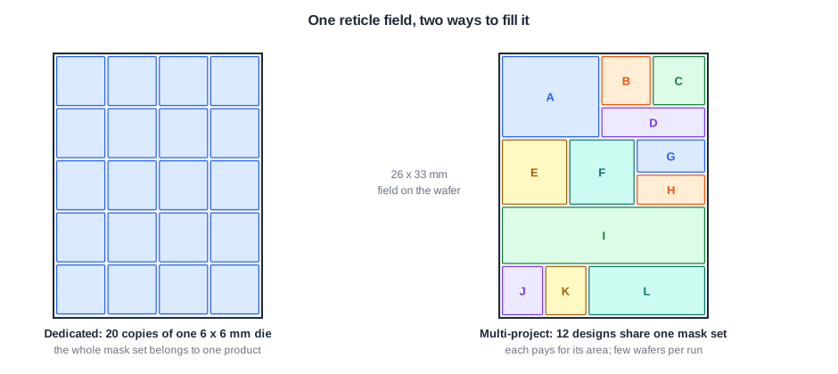
- A dedicated mask set. The reticle holds as many copies of one die as fit in the exposure field, often with a few test structures. Every wafer of the run carries only this product. This is the route for production: the mask cost is spread over thousands of wafers.
- A multi-project wafer (MPW). One reticle holds many different designs, each in a slot of the size it paid for. The mask cost is split between them, and a run produces only a few wafers. Each customer receives a small number of its own dies. University programmes, prototyping services and open-source shuttles work this way.
An MPW is cheap per project but has limits. There are fixed tapeout dates, the die size is set by the slot, the yield is not representative because so few wafers are made, and the process options are those the shuttle offers. A product moves to its own mask set once the design is proven.
Shuttles for small digital blocks go further and share the chip itself. TinyTapeout, used in Project: A TinyTapeout Tile, places each project in a tile of a common chip with a shared pad ring and a multiplexer that selects one project at a time. The designer delivers only the tile; pads, seal ring, fill and the chip-level sign-off come from the shuttle.
Quick Check
Q: A start-up has a working prototype from an MPW run and now needs 50,000 parts. Why does it usually order a dedicated mask set rather than more MPW runs?
Show Answer
An MPW run produces only a few wafers, and each carries only a few of its dies, so the cost per die stays high and the supply is tied to the shuttle schedule. A dedicated mask set puts many copies of the die on every field and can run as many wafers as needed; its one-time cost is spread over the whole volume.
Running It in ChipVerify Lab
Run Place and Route on the multiplier and download the GDSII from the report. Open it in KLayout and list the layers: you should find the drawing layers from n-well to met5, the pin and label layers, and the placement boundary, but no pad openings, no seal ring and no fill. The report's DRC and LVS sections are the kind of evidence that goes into a tapeout package. With PRO, the TinyTapeout mode builds the same design as a shuttle tile, the form in which a block like this can actually reach silicon.
Common Mistakes
Mistake #1: Treating the GDSII as the whole tapeout
Process options, layer map, PDK version and die facts travel with the file. A missing option can make a correct layout useless.
Mistake #2: Signing off with an old rule deck
The foundry checks with its current deck. Re-run DRC with the latest deck before tapeout, or expect the review to bounce the design.
Mistake #3: Expecting production yield data from an MPW
A few wafers and a few dies each say whether the design works, not how well it yields across lots.
Practice Exercise
Challenge: Sharing a Mask Set
A multi-project reticle has 200 die sites. Twenty projects share it, each taking the same number of sites. How many dies of its own does each project get per wafer, and what share of the mask cost does each pay? If a full mask set costs $1 million, what is each project's share?
Hint
Divide the sites, then divide the cost, by the number of projects.
Solution
200 / 20 = 10 dies per project on each wafer, and each project pays 1/20 of the mask cost: $1,000,000 / 20 = $50,000. In practice MPW prices are set per area, so a larger slot pays more.
Open the ready-made example in the lab, synthesize it and run Place and Route.
Summary
- A tapeout package holds the GDSII or OASIS file, the process and its options, the layer map, the PDK version, sign-off reports with waivers, die facts and the list of third-party IP.
- The foundry re-runs DRC with its own deck, checks the form against the file, and merges the die into a frame with scribe lanes, marks and test modules.
- The customer approves the framed result before mask data preparation begins.
- The lab multiplier is a clean block with 34 layer and datatype pairs, but no pads, seal ring, fill or chip ID.
- A dedicated mask set suits production; a multi-project wafer shares the mask cost for prototypes and education.