
The technology LEF tells a place and route tool what the process looks like: the units, the placement site, every routing and cut layer with its direction, pitch, width and spacing rules, and the vias that connect the layers. The router uses it to know where wires may go and how close they may be, and the extractor uses it to estimate their resistance and capacitance. This article reads the sky130 technology LEF section by section.
8 min read | Beginner to Intermediate
What You'll Learn
- Read the units, manufacturing grid and site definitions of a technology LEF
- Interpret a routing layer: direction, pitch, width, spacing and area rules
- Understand via definitions and via generation rules
- Find the electrical data: resistance, capacitance, current density and antenna ratios
Units, Grid and Sites
UNITS
  TIME NANOSECONDS 1 ;
  CAPACITANCE PICOFARADS 1 ;
  RESISTANCE OHMS 1 ;
  DATABASE MICRONS 1000 ;
END UNITS

MANUFACTURINGGRID 0.005 ;

SITE unithd
  SYMMETRY Y ;
  CLASS CORE ;
  SIZE 0.46 BY 2.72 ;
END unithd
DATABASE MICRONS 1000 means that coordinates in DEF and in the tool database are integers in nanometres. MANUFACTURINGGRID 0.005 means every shape edge must fall on a 5 nm grid: a strap at an offset of 3.278 um is illegal, 3.280 um is fine. The site unithd is the 0.46 x 2.72 um placement unit of the high-density cells. A second site, unithddbl, is twice as tall for double-height cells.
Routing Layers
Each routing layer is a block like this one for met1:
LAYER met1
  TYPE ROUTING ;
  DIRECTION HORIZONTAL ;
  PITCH 0.34 ;
  OFFSET 0.17 ;
  WIDTH 0.14 ;
  SPACINGTABLE
     PARALLELRUNLENGTH 0
     WIDTH 0 0.14
     WIDTH 3 0.28 ;
  AREA 0.083 ;
  THICKNESS 0.35 ;
  ANTENNAMODEL OXIDE1 ;
  ANTENNADIFFSIDEAREARATIO PWL ( ( 0 400 ) ( 0.0125 400 ) ( 0.0225 2609 ) ( 22.5 11600 ) ) ;
  EDGECAPACITANCE 40.567E-6 ;
  CAPACITANCE CPERSQDIST 25.7784E-6 ;
  DCCURRENTDENSITY AVERAGE 2.8 ;
  MAXIMUMDENSITY 70 ;
  DENSITYCHECKWINDOW 700 700 ;
  RESISTANCE RPERSQ 0.125 ;
END met1
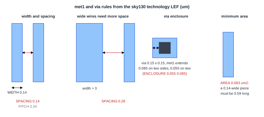
Reading it from the top:
- DIRECTION, PITCH, OFFSET: routing tracks run horizontally, 0.34 um apart, the first one 0.17 um from the origin.
- WIDTH: the minimum wire width, 0.14 um.
- SPACINGTABLE: the minimum spacing depends on the wire width: 0.14 um normally, 0.28 um next to a wire wider than 3 um. Wide wires, such as power straps, need more room.
- AREA: every isolated piece of met1 must be at least 0.083 um2. A 0.14 um wide stub must be about 0.59 um long.
- THICKNESS, RESISTANCE, CAPACITANCE: data for estimating wire RC. The sheet resistance is 0.125 ohm per square.
- DCCURRENTDENSITY: the maximum average current, 2.8 mA per micron of width at 90 C, for electromigration checks.
- MAXIMUMDENSITY: at most 70 % of any 700 x 700 um window may be met1, a rule for even polishing during manufacturing.
- ANTENNA lines: how much metal may connect to a transistor gate before the antenna effect damages it. See The Antenna Effect.
Quick Check
Q: Two met1 wires run side by side. One is a 4 um wide power strap, the other a minimum-width signal. What is the minimum spacing between them?
Show Answer
0.28 um. The spacing table applies the wider value because one of the wires is wider than 3 um. Two minimum-width wires need only 0.14 um.
Cut Layers and Vias
Cut layers hold the via holes. The rules for via, the cut between met1 and met2:
LAYER via
  TYPE CUT ;
  WIDTH 0.15 ;
  SPACING 0.17 ;
  ENCLOSURE BELOW 0.055 0.085 ;
  ENCLOSURE ABOVE 0.055 0.085 ;
  DCCURRENTDENSITY AVERAGE 0.29 ;
END via
A via cut is 0.15 um square, two cuts must be 0.17 um apart, and the metal above and below must extend past the cut by 0.055 um on two opposite sides and 0.085 um on the other two. Each cut carries at most 0.29 mA, which is why power connections use arrays of cuts.
The LEF then defines ready-made vias. M1M2_PR is the default met1-to-met2 via:
VIA M1M2_PR DEFAULT
  LAYER via ;
  RECT -0.075 -0.075 0.075 0.075 ;
  LAYER met1 ;
  RECT -0.16 -0.13 0.16 0.13 ;
  LAYER met2 ;
  RECT -0.13 -0.16 0.13 0.16 ;
END M1M2_PR
A VIARULE ... GENERATE with the same name tells the tool how to build larger via arrays, as the power grid needs. The sky130 technology LEF defines 25 fixed vias. In a routed DEF you see their names at every layer change, such as M1M2_PR or L1M1_PR_MR.
Quick Check
Q: The met1 shape of M1M2_PR is 0.32 by 0.26 um. Where do these numbers come from?
Show Answer
From the cut and the enclosure: 0.15 + 2 x 0.085 = 0.32 um in one direction and 0.15 + 2 x 0.055 = 0.26 um in the other.
What the LEF Does Not Contain
The technology LEF is a simplified view of the rules. The full design rule manual has hundreds of rules the router does not need, such as rules for diffusion, poly and implants, which only matter inside the cells. Those are checked by the DRC deck at sign-off. A layout that the router considers clean can still fail DRC, which is why Design Rule Checking is a separate step.
Some electrical data can also be missing. The sky130 technology LEF used by the lab has no resistance values for the vias, which the IR drop analysis needs; the flow supplies them separately with set_layer_rc -via.
Running It in ChipVerify Lab
Run Place and Route on the counter and look at the routing in the layout viewer: the met1 wires lie on horizontal tracks 0.34 um apart and the met2 wires on vertical tracks 0.46 um apart, and every corner has a via.
Common Mistakes
Mistake #1: Assuming a clean route means a clean layout
The router only knows the rules in the technology LEF. Sign-off DRC with the full rule deck is still required.
Mistake #2: Placing shapes off the manufacturing grid
Custom power straps, pins or blockages must use coordinates on the 5 nm grid. OpenROAD stops with an error when a strap offset does not fit the grid.
Practice Exercise
Challenge: Tracks per Row
A standard cell row is 2.72 um tall. How many met1 routing tracks cross one row? How many met2 tracks cross a 7.36 um wide flip-flop?
Hint
Divide the length by the pitch of the layer that runs across it.
Solution
2.72 / 0.34 = 8 horizontal met1 tracks per row height. 7.36 / 0.46 = 16 vertical met2 tracks over the flip-flop. Some of the met1 tracks are taken by the power rails at the row edges, and the cell's own pins block a few more.
Open the ready-made example in the lab, synthesize it and run Place and Route.
Summary
- The technology LEF defines units (1000 per micron), the manufacturing grid (5 nm) and placement sites.
- Each routing layer has a direction, pitch, width, width-dependent spacing, minimum area and RC data.
- Cut layers define via sizes, spacing and enclosure; fixed vias and via rules build the connections.
- It also holds current-density, density and antenna rules, but not the full design rule manual.
