
Everything in the earlier chapters happened inside one block: a die area, a core, rows of standard cells and a power grid fed from straps at the edge. A real chip adds a layer around all of that. It needs I/O cells that drive signals off the die and protect it from static discharge, pads or bumps where the package connects, supply pads that bring current in, and a top-level floorplan that places the blocks inside the pad ring. This article describes what the top level adds, using the open Caravel harness chip, built in sky130, as a real example with real dimensions.
7 min read | Intermediate
What You'll Learn
- Name what a full chip has that a block does not
- Read a chip-level floorplan: pad ring, core, blocks and supply domains
- Describe the order of the chip-level steps
- Explain why I/O and package decisions are made early
Block Versus Chip
In the lab, the multiplier's pins are simply metal shapes on the die edge, and the power grid's straps are assumed to be fed from outside. That is the right model for a block that will sit inside a larger chip. Its pins connect to other blocks' wires, and its supply comes from the parent's grid.
A chip has nothing outside it except the package. Every signal that leaves it must be driven strongly enough to charge a board trace, at a voltage another chip understands. Every input must survive whatever the outside world applies to it, including electrostatic discharge from a person or a machine. All the supply current has to enter through a limited number of connections. These jobs are done by components that a block never sees:
- I/O cells. Large cells with output drivers, input receivers, level shifters and ESD protection, described in I/O Cells: Drivers, Receivers and Level Shifting.
- The pad ring. I/O cells, supply pads, corner cells and filler cells placed edge to edge around the die, forming continuous supply buses. See Building the Pad Ring.
- Pads or bumps. The metal openings where bond wires or solder bumps attach.
- Supply pads and their placement. How many are needed and where, covered in Power and Ground Pads: How Many and Where.
- The package. Its connections and parasitics feed back into the floorplan, as Chip-Package Co-Design explains.
A Real Chip: Caravel
Caravel is the harness chip that carries user designs on the open sky130 shuttles. Its layout is public, so its numbers can be read directly from the design files: the die is 3,588 x 5,188 um, or 18.6 mm2.

The floorplan has three parts:
- The pad ring around the edge, about 200 um deep: the sky130 I/O cells are 200 um tall, and the corner cells 200 x 204 um. The core inside it is 3,165 x 4,767 um, so the ring takes 3.5 mm2, 19 % of the die.
- The management area at the bottom of the core: a small processor with its memories, a housekeeping block, clocking and a power-on reset.
- The user area, 2,920 x 3,520 um, which is 55 % of the die. A user's design is hardened as one block of exactly this size, with its pins at fixed positions on its edges.
For a user of Caravel, the user area is just a block with a fixed outline and fixed pins, like the blocks of Hierarchical Physical Design. Caravel's own designers did the chip-level work: the pad ring, the routing from the ring to the user area, the supply domains and the package.
Quick Check
Q: In Caravel, the pad ring takes 19 % of the die. Would that share be larger or smaller on a chip of the same pad count but four times the area?
Show Answer
Smaller. The ring is a band of fixed depth around the edge, so its area grows with the perimeter, while the die area grows with the square of the side. Doubling the side doubles the ring area but quadruples the die area, roughly halving the ring's share. That is why the ring matters most on small dies.
Supply Domains at the Chip Level
A block has one VDD and one VSS. A chip usually has several supplies, and the pad ring carries them all. Caravel's pinout lists:
| Supply | Voltage | Feeds |
|---|---|---|
| vddio | 3.3 V | the I/O drivers, ESD protection and the pad ring |
| vccd, vdda | 1.8 V, 3.3 V | the management area, digital and analog |
| vccd1, vdda1 | 1.8 V, 3.3 V | user area 1 |
| vccd2, vdda2 | 1.8 V, 3.3 V | user area 2 |
| vssio, vssa, vssd and the user grounds | 0 V | matching grounds |
The core logic runs at 1.8 V on thin-oxide transistors, while the I/O runs at 3.3 V on thick-oxide transistors that tolerate it. Separate supplies also keep the noise of switching outputs away from the core, and the noise of digital logic away from analog circuits. Each domain needs its own supply pads, its own segment of bus in the pad ring, and ESD protection between it and every other domain.
The Chip-Level Steps
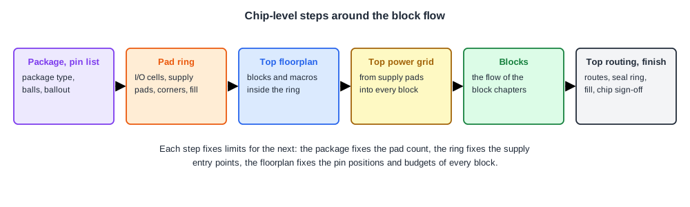
- Package and pin list. The package type, its number of pins or balls, and which signal and supply goes where. This comes first because it fixes how many pads the die needs and on which side.
- Pad ring. I/O cells and supply pads in their slots, corners, fillers, and the bond pads or bumps.
- Top floorplan. Blocks and macros placed inside the ring, close to the I/Os they use, with channels for top-level routing.
- Top power grid. Rings and straps from the supply pads to the core and into every block's own grid.
- Blocks. Each block is implemented as in the earlier chapters, with pin positions and timing budgets from the top level.
- Top-level routing and chip finishing. Routes between blocks and to the I/O cells, then seal ring, fill, logos and the final checks of Physical Sign-Off Checklist, run on the full chip.
The order matters because each decision limits the next. A package with too few balls cannot be fixed by the floorplan, and a pad ring with too few supply pads cannot be fixed by the power grid.
Quick Check
Q: A team finishes all its blocks and only then chooses a package, and the package has fewer supply balls than the chip has supply pads. What are the options, and why are they all bad?
Show Answer
Several supply pads must share a ball, which raises the inductance and IR drop of that supply, or the team must choose a larger, more expensive package, or remove supply pads, which weakens the power delivery the grid was designed for. Each option undoes earlier work. Choosing the package and pin list first avoids the problem.
What Changes for the Physical Designer
Several topics from the block chapters look different at the top level:
- Pin placement becomes pad placement. A block pin can move by a few micrometres; an I/O cell moves in slots of its own width, and its position is tied to the package.
- The power grid starts at the supply pads, not at an assumed source. The IR drop of IR Drop: Static and Dynamic includes the path from pad to block, and the pad count and spacing become design variables.
- Timing includes the I/O cells, whose delays depend on the board load, and the long top-level routes between blocks.
- Verification adds checks that only make sense for a chip: ESD paths for every pad, latch-up rules near the I/O, and a full-chip LVS that includes the pad cells.
Running It in ChipVerify Lab
At the time of writing, the lab's Place and Route flow implements a block: it has no I/O cell library, pad ring or bumps. The articles of this chapter use the sky130 I/O library files and the public Caravel layout as their data. With PRO, you can still prepare a block for a fixed-outline slot like Caravel's user area: set the die area in the panel and keep the pins on the edges where the parent expects them.
Common Mistakes
Mistake #1: Treating the chip as one big block
A chip needs I/O cells, supply pads, ESD protection and a package; a block flow provides none of them.
Mistake #2: Choosing the package last
The package fixes the pad count and the supply connections. Choose it before the floorplan.
Mistake #3: Forgetting the ring's area
On a small die, the pad ring can take a fifth of the area or more. Include it in the die size estimate from the start.
Practice Exercise
Challenge: Size a Small Chip
A design's core logic needs 2.0 x 2.0 mm. It will sit inside a pad ring 200 um deep, like Caravel's. What is the die size and what share of the die does the ring take? How does that change if the core is 4.0 x 4.0 mm?
Hint
Add the ring depth on both sides of the core.
Solution
Die side 2.0 + 2 x 0.2 = 2.4 mm, die area 5.76 mm2, core 4.0 mm2, so the ring takes 1.76 mm2, 31 %. With a 4.0 mm core: die 4.4 mm, 19.36 mm2, ring 3.36 mm2, 17 %. The ring's share falls as the chip grows, assuming the pads still fit on the perimeter.
Summary
- A chip adds I/O cells, a pad ring, pads or bumps, supply pads and a package to the block flow.
- Caravel's die is 3,588 x 5,188 um; its pad ring takes 19 % of the die and its user area 55 %.
- Chips have several supply domains, for core, I/O and analog, each with its own pads and ring bus.
- The chip-level steps run from package and pin list to pad ring, floorplan, power grid, blocks, routing and chip-level sign-off.
- Package and pad decisions come first because later steps cannot undo them.
