
The RTL-to-GDSII flow is the chain of steps that takes a Verilog description and produces the GDSII file a foundry turns into masks. Front-end steps such as synthesis decide the logic. Back-end steps, physical design, decide the geometry. This article walks one small design, an 8-bit counter, through every step of the flow ChipVerify Lab runs, and shows what each step adds, with a picture of the layout after each one.
8 min read | Beginner
What You'll Learn
- List the steps from RTL to GDSII in order
- Describe what each step adds to the design
- Match each step to the OpenROAD command that performs it
- Read a layout picture at each stage of the flow
The Steps and Their Commands
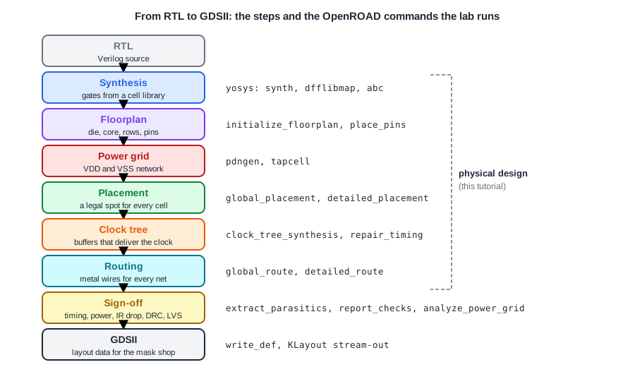
Each box is a step, and next to it is the command that does it in the lab's flow. Commercial tools use different command names, but the order is the same. Synthesis is not part of physical design, but it produces the netlist that physical design starts from, and its choice of cells affects everything afterwards.
The design used here is a plain 8-bit counter with an enable and a synchronous reset:
module counter8 (
  input            clk,
  input            rst,
  input            en,
  output reg [7:0] q
);
  always @(posedge clk) begin
    if (rst)
      q <= 8'd0;
    else if (en)
      q <= q + 8'd1;
  end
endmodule
Synthesis with the sky130 high-density library maps it to 28 cells: 8 dfxtp_1 flip-flops and 20 logic gates, 280.3 um2 in total. The clock period is 5 ns and the target utilization 50 %.
One Design, Four Snapshots
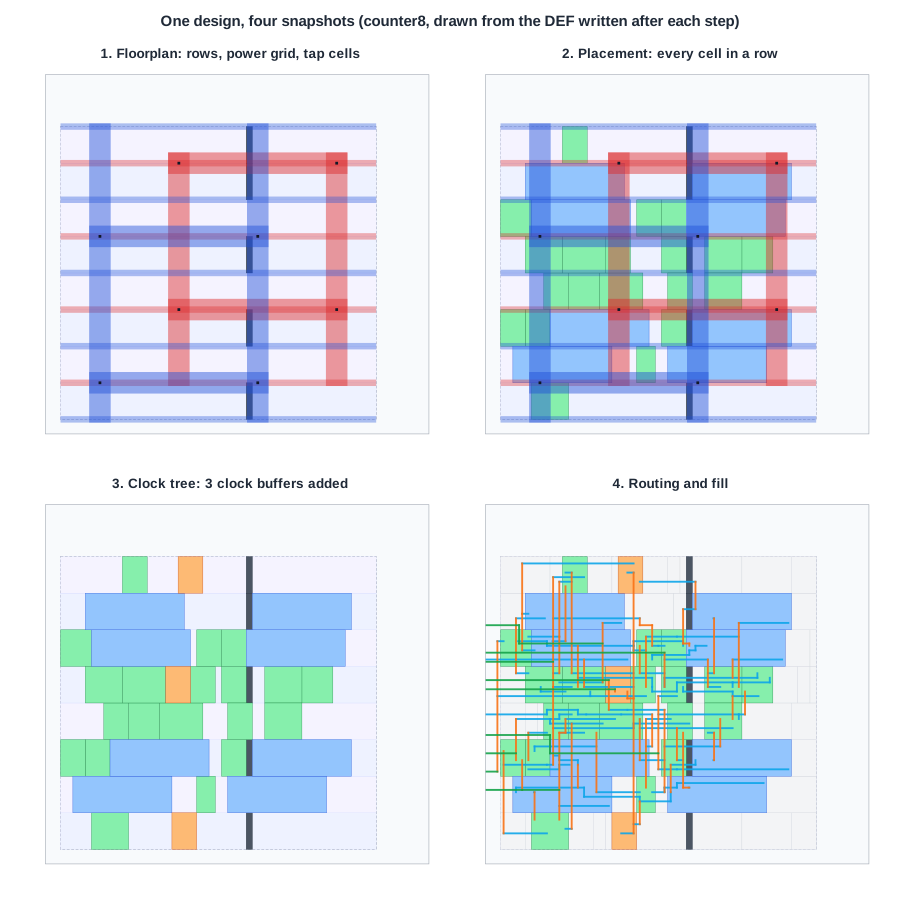
1. Floorplan
initialize_floorplan sizes the core from the cell area and the utilization, and fills it with rows of placement sites: 8 rows, 23.5 um wide. place_pins puts the 11 I/O pins on the die edge. Then pdngen builds the power grid: thin rails along every row edge on met1, and vertical and horizontal straps on met4 and met5. tapcell adds five tap cells (dark grey) that tie the wells to the supplies. No logic cell has a position yet.
2. Placement
global_placement spreads the cells over the core so that connected cells are close, while keeping the density near the target. detailed_placement then snaps every cell into a row on a legal site with no overlaps. The blue boxes are the eight flip-flops, the green boxes are logic gates.
3. Clock Tree Synthesis
clock_tree_synthesis builds a tree of buffers from the clock pin to the eight flip-flops. For this small design it adds three clkbuf_2 cells (orange): one root buffer driving two leaf buffers, each feeding four flip-flops. After CTS, repair_timing checks setup and hold timing with the real clock and finds nothing to fix.
4. Routing
global_route plans a coarse path for every net, and detailed_route draws the actual wires on the routing tracks: here mostly met1 (horizontal, blue) and met2 (vertical, orange), with short met3 wires (green) to the pins on the left edge. Finally filler_placement fills every empty site with filler cells (light grey), so the rows are continuous.
Quick Check
Q: Why does clock tree synthesis come after placement, and routing after CTS?
Show Answer
CTS needs to know where the flip-flops are, so it can build a balanced tree to their real positions. The clock buffers then need their own place in the rows. Routing comes last because it must connect every cell, including the ones CTS added, at their final positions.
Sign-Off and GDSII
After routing, the flow extracts the wire parasitics and checks the result:
- Timing: with propagated clocks and the extracted wire RC, the worst setup slack of the counter at 5 ns is +3.31 ns.
- Power:
report_powergives about 105 uW, of which the clock network is about a third. - IR drop:
analyze_power_gridcomputes the voltage drop in the VDD and VSS grids. - Antenna, DRC and LVS: checks that the layout follows the manufacturing rules and matches the netlist. For the counter, all three are clean.
The layout is written as DEF, converted to GDSII with KLayout by merging in the cell layouts, and the GDSII is what goes to the foundry. The GDSII Out and Tapeout article covers the last step in detail.
Quick Check
Q: The flow checks timing after routing. Is the timing check after synthesis wasted effort?
Show Answer
No. Synthesis timing catches paths that are hopeless before any layout work is spent on them, and it guides the choice of cells. But it uses estimated wires and an ideal clock, so it is a prediction. Post-route timing is the real check.
Running It in ChipVerify Lab
The example is the counter from this article. Synthesize it, then run Place and Route with the default settings. The layout viewer shows the final layout; the report has a section for each step: area and floorplan, CTS, timing, power, IR drop, antenna, DRC and LVS. The LVS section compares the layout with the netlist, as explained in Layout Versus Schematic (LVS).
Common Mistakes
Mistake #1: Changing the netlist after placement without re-running the later steps
Every step depends on the ones before it. A new cell needs a position, new clock sinks need the tree rebuilt, and new nets need routing. Changes late in the flow are made as ECOs that update only what is needed.
Mistake #2: Ignoring warnings from early steps
A floorplan that is too small or a power grid with gaps does not stop the flow at once, but it causes routing failures or timing problems much later. Read the log of every step.
Practice Exercise
Challenge: Double the Counter
Change the counter to 16 bits (output reg [15:0] q, and 16-bit constants), synthesize it and run Place and Route at 5 ns. Before running, predict how the cell area, the number of tap cells and the worst slack change.
Hint
The carry chain gets longer, and the core grows with the cell area.
Solution
The 16-bit counter has 16 flip-flops and 43 logic gates. The design area doubles from 302 to 604 um2, the die grows from 43.7 um to 53.6 um per side, and the bigger core needs 14 tap cells instead of 5. CTS still builds a three-buffer tree, now with stronger clkbuf_4 cells for 16 sinks. The worst setup slack drops from +3.31 ns to +2.46 ns, because the longer carry chain makes the critical path slower.
Open the ready-made example in the lab, synthesize it and run Place and Route.
Summary
- The RTL-to-GDSII flow runs synthesis, floorplan, power grid, placement, CTS, routing and sign-off, then writes GDSII.
- The floorplan defines the core, rows and pins; the power grid and tap cells come next.
- Placement positions the cells, CTS adds clock buffers, routing adds the metal wires, and fillers complete the rows.
- Sign-off checks timing, power, IR drop, antenna rules, DRC and LVS with the real layout.
