
The pad ring is the band of I/O cells, supply pads, corner cells and filler cells around the edge of a chip. Its cells sit edge to edge so that their supply buses join into continuous rings, and every signal and supply that enters or leaves the die passes through one of its slots. This article builds the ring step by step, reads the real ring of the Caravel chip from its layout files, shows the OpenROAD commands that place one, and works out when the ring, not the logic, sets the size of the die.
8 min read | Intermediate
What You'll Learn
- List the cells of a pad ring and the role of each
- Describe how supply buses are formed and split by abutment
- Read the pad placement commands of OpenROAD
- Decide whether a die is pad-limited or core-limited
The Cells of a Ring
A ring is built from four kinds of cells, all from the I/O library:
- Signal I/O cells, such as the sky130 GPIO cell of I/O Cells: Drivers, Receivers and Level Shifting, 80 um wide.
- Supply pads for every supply and ground, 75 um wide in sky130, most of them with an ESD clamp.
- Corner cells, 200 x 204 um in sky130, which turn every supply bus through 90 degrees.
- Filler slices, which carry the buses across the gaps between pads. sky130's are 1, 5, 10 and 20 um wide, so any gap that is a whole number of micrometres can be filled exactly.
The supply buses run across every one of these cells on the upper metals, at the same height in each. Placed edge to edge, the cells form rings of VDDIO, VSSIO, VCCD, VSSD and the other supplies all the way around the die, without a single routed wire. A missing filler leaves a gap in every bus at once, which is why the ring must be closed before anything else is checked.
Caravel's Ring, Read From Its Layout
Caravel's padframe is published as a DEF file with 818 components. Leaving out seven small constant-value blocks, the ring contains:
| Cell type | Count |
|---|---|
| GPIO cells (80 um) | 44 |
| Supply pads with ESD clamps (75 um) | 18 |
| Reset input with glitch filter | 1 |
| Corner cells | 4 |
| Filler slices (1, 5, 10, 20 um) | 669 |
| Slices that join or split particular buses | 75 |
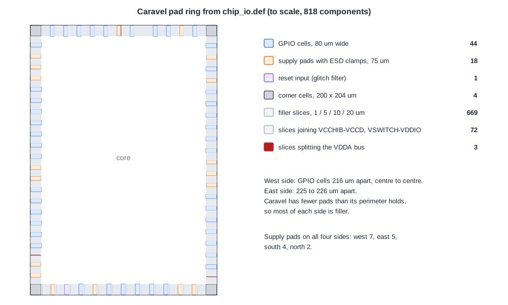
Three things are visible in the drawing:
- Pads are spread out. On the west side, the GPIO cells sit 216 um apart, centre to centre, although each is only 80 um wide. Caravel has fewer pads than its perimeter could hold, so most of each side is filler.
- Supply pads are distributed. The 18 supply pads sit on all four sides, so every part of the ring has a supply connection nearby.
- Buses are deliberately split. Three slices disconnect the VDDA bus, splitting the analog supply into separate segments for different parts of the chip. Another 72 slices connect particular buses to each other, VCCHIB to VCCD and VSWITCH to VDDIO, where the design needs them joined.
Quick Check
Q: A designer replaces a 20 um filler slice with a 20 um gap to make room for a top-level route. What breaks?
Show Answer
Every supply bus in the ring is interrupted at that point, because the filler carried all of them. The pads on either side lose their connection to each other's supplies, and the ESD discharge paths that rely on the continuous bus are cut. Routes to the core must cross the ring through the I/O cells' own core-side pins, not through gaps.
Building a Ring in OpenROAD
OpenROAD's pad module, based on the ICeWall tool, places a ring in a fixed order. The commands below are from its documentation; the cell names are sky130's. This flow is not available in the lab at the time of writing.
# rows for the I/O cells along the four edges, and the corner sites
make_io_sites -horizontal_site IOSITE_H -vertical_site IOSITE_V \
              -corner_site IOSITE_C -offset 0

# corner cells first
place_corners sky130_ef_io__corner_pad

# signal and supply pads at chosen positions (um along the row)
place_pad -row IO_SOUTH -location 600.0 {u_gpio_0}
place_pad -master sky130_ef_io__vccd_lvc_clamped_pad \
          -row IO_SOUTH -location 900.0 {u_vccd_0}

# fill every remaining gap, widest slices first
place_io_fill -row IO_SOUTH sky130_ef_io__com_bus_slice_20um \
    sky130_ef_io__com_bus_slice_10um sky130_ef_io__com_bus_slice_5um \
    sky130_ef_io__com_bus_slice_1um

# join the supply buses of neighbouring cells into rings
connect_by_abutment
make_io_sitescreates the rowsIO_NORTH,IO_SOUTH,IO_EASTandIO_WEST. If the library has no I/O sites,make_fake_io_sitedefines them.place_padputs an existing instance, or a new one of the given master, at a location along the row.place_padscan spread a list of pads automatically.place_io_fillis the ring's equivalent of filler cells in the core, from Filler Cells, Metal Fill and Density Rules.connect_by_abutmentturns the touching bus shapes into connected nets in the database, so the power grid and LVS see the rings.- For libraries whose I/O cells have no pad of their own,
place_bondpadadds a bond pad over each cell. sky130's cells already contain their pad on met5.
After the ring, the top-level power grid connects the core supply rings to the supply pads' core-side pins, and the router connects each I/O cell's core-side pins to the logic.
Pad-Limited or Core-Limited
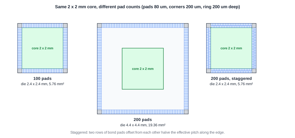
The ring needs room for all its pads. Take a core of 2 x 2 mm, a ring 200 um deep, corner cells 200 um wide and pads butted at 80 um, with no fillers between them:
| Pads | Die side needed by the pads | Die side needed by the core | Die | Limited by |
|---|---|---|---|---|
| 40 | 1.2 mm | 2.4 mm | 2.4 x 2.4 mm, 5.76 mm2 | core |
| 100 | 2.4 mm | 2.4 mm | 2.4 x 2.4 mm, 5.76 mm2 | both |
| 200 | 4.4 mm | 2.4 mm | 4.4 x 4.4 mm, 19.36 mm2 | pads |
The pad side is 25 pads x 80 um plus two corners for 100 pads, and 50 pads x 80 um plus two corners for 200. At 200 pads the die is more than three times larger than the logic needs, and the extra area is empty. Such a chip is called pad-limited: its size is set by the pad frame rather than by its logic.
A pad-limited design has several ways out:
- Staggered pads. Two rows of bond pads, offset from each other, halve the effective pitch along the edge. In the example, 200 pads at an effective 40 um fit on a 2.4 mm die again. The cost is longer bond wires and a greater risk of wires touching. OpenROAD supports this through offsets in
place_bondpad. - Narrower I/O cells, if the library offers them, with lower drive strength.
- Flip-chip. Bumps over the whole die area remove the perimeter limit, as Flip-Chip: Bump Maps and RDL Routing shows.
- Fewer pins, by serializing interfaces or sharing pins.
A core-limited chip has the opposite situation: spare slots. These are filled with filler slices, or used for extra supply pads, which lower the supply inductance for free.
Quick Check
Q: A pad-limited chip has a large empty area inside its ring. Why is adding more logic to that area almost free, while adding more pads is expensive?
Show Answer
The die size is fixed by the pads, so logic that fits inside the existing ring adds no area, only a little power. Each extra pad, on the other hand, lengthens the ring and therefore every side of the die, and the die area grows with the square of the side.
Where Each Pad Goes
Pad order is not arbitrary. The package fixes which side each signal can reach, as Chip-Package Co-Design explains. Inside that freedom, designers keep a bus's pads together and in bit order, place each interface's pads next to the block that uses it to shorten top-level routes, put supply pads among groups of outputs, and keep sensitive analog pads away from fast digital outputs. The number and spacing of supply pads is the subject of Power and Ground Pads: How Many and Where.
Running It in ChipVerify Lab
At the time of writing, the lab's flow does not place I/O cells or a pad ring; its pins are block pins on the die edge, as in I/O Pin Placement. The numbers above come from the Caravel padframe DEF, the sky130 I/O LEF files and the calculation of the table.
Common Mistakes
Mistake #1: Leaving gaps in the ring
Every gap breaks every supply bus. Fill each row completely and check bus continuity in LVS.
Mistake #2: Joining buses that must stay separate
Supplies of different domains, or quiet analog grounds, need their bus segments split. Use the library's disconnect slices where the domains change.
Mistake #3: Discovering pad limitation late
Count pads, including supply pads, against the perimeter at the start. Changing the die size after the floorplan is expensive.
Practice Exercise
Challenge: Fit 120 Pads
A chip needs 120 pads: 88 GPIO cells at 80 um and 32 supply pads at 75 um. Corners are 200 um, the ring is 200 um deep and the core needs 2.0 x 2.0 mm. Distributing the pads evenly over four sides, is the chip pad-limited? What is the smallest square die?
Hint
Each side holds 22 GPIO cells and 8 supply pads.
Solution
One side needs 22 x 80 + 8 x 75 = 1,760 + 600 = 2,360 um of pads plus 2 x 200 um of corners: 2,760 um. The core needs 2,000 + 2 x 200 = 2,400 um. The pads win, so the chip is pad-limited with a 2.76 mm die, 7.6 mm2 instead of 5.76 mm2.
Summary
- A pad ring holds signal I/O cells, supply pads, corner cells and filler slices placed edge to edge.
- Supply buses run through every ring cell and join by abutment; special slices split or join particular buses.
- Caravel's ring has 44 GPIO cells, 18 supply pads, a reset pad, 4 corners and 744 slices.
- OpenROAD places a ring with make_io_sites, place_corners, place_pad, place_io_fill and connect_by_abutment.
- A chip whose pads need more perimeter than its core is pad-limited; staggered pads, narrower cells or flip-chip help.
