
A photomask is a quartz plate with a chrome pattern that the fab projects onto the wafer to define one layer of the chip. Every mask layer of the process needs its own mask, and none of them is a plain copy of a layer in the GDSII. Between tapeout and the first exposure, mask data preparation turns the drawn layers into mask layers, adds fill, corrects the shapes for the optics that will print them, and cuts them into pieces a mask writer can draw. This article follows that path with the sky130 mask list and the GDSII of the routed multiplier from the lab.
7 min read | Intermediate
What You'll Learn
- Distinguish drawn layers from mask layers
- Explain why masks are corrected with OPC and other resolution enhancements
- Describe fracturing, mask writing, inspection and the pellicle
- Relate mask cost to the number and type of mask layers
Drawn Layers and Mask Layers
The layers in a GDSII file are drawn layers: what the designer or the standard cell library drew. The masks are process layers: what the fab exposes, step by step. The two lists overlap but are not the same.
The routed multiplier from the lab has shapes on 20 drawing layers plus pin, label, marker and boundary layers. The sky130 PDK documentation lists the masks of SkyWater's 130 nm processes and marks 34 of them as used in sky130. Matching the two by name gives this picture:
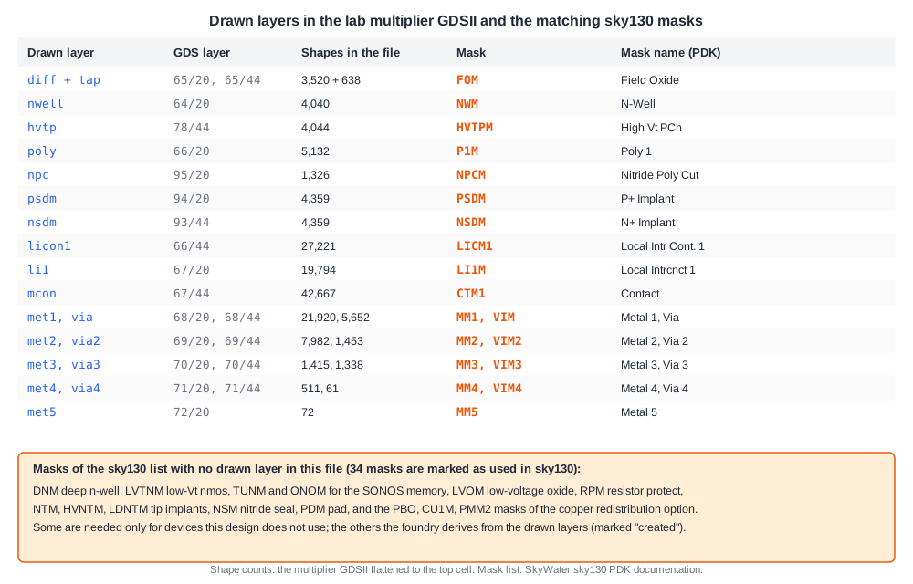
Three things stand out:
- Different names for the same idea. The drawn layers diff and tap, the active areas of transistors and taps, correspond to the mask called Field Oxide (FOM): the mask defines where active silicon is and, by its complement, where the isolation oxide goes. The drawn contact layer mcon is printed by the mask simply called Contact (CTM1).
- Masks with no drawn layer. Tip implants, a nitride seal, pad openings and the masks of the copper redistribution option have no shapes in a block GDSII. Some belong to devices or options this design does not use. Others are generated by the foundry's mask data preparation from the drawn layers; the PDK's layer tables mark such layers as "created" rather than "drawn", with the note that they are only created by CAD.
- Fill and dummies. The foundry adds its own fill shapes to some masks, for example dummy active areas, to even out density. The sky130 layer tables list a "FOM dummy" layer for exactly this.
The lesson for a physical designer is that DRC is written in terms of drawn layers, but the fab builds mask layers. The rule deck encodes the relation between the two, which is why a rule that seems strange in the layout often makes sense as a mask or process limit.
Correcting for the Optics: OPC
The scanner projects the mask through lenses onto photoresist. When the features are close to or smaller than the wavelength of the light, the image is blurred by diffraction: corners round, line ends pull back, and narrow isolated lines print differently from the same lines in a dense array. This optical proximity correction (OPC) became necessary at the 180 nm node and is in heavy use at 45 nm.
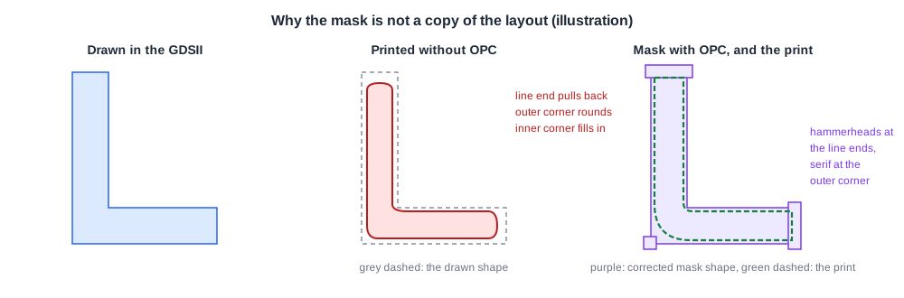
OPC changes the mask shapes so that the printed result matches the drawn one: it adds hammerheads to line ends so they reach their drawn length, serifs to outer corners, notches to inner corners, and moves edges according to their neighbourhood. Early OPC used rules; modern OPC simulates the printing of every edge and moves it until the simulated print is on target.
OPC is one of several resolution enhancement techniques (RET). Others change the light itself: phase-shift masks vary the thickness of the quartz so that light from neighbouring openings cancels between them, and off-axis illumination tilts the light to improve contrast for dense, repeated patterns. At the finest pitches a single mask is not enough, and one layer is split over two or more masks, as Advanced Nodes described.
Quick Check
Q: A designer draws a met1 line end exactly at the minimum extension past a via. Why is it the mask, not the layout, that gets the hammerhead?
Show Answer
The layout describes the intended result on the wafer, and DRC checks that intent. The pull-back of line ends is a property of the optics and the resist, which the foundry models. Correcting the mask keeps the design rules simple and lets the foundry update the correction when its process changes, without touching the design.
Fracturing and Writing the Mask
The corrected data still has to be drawn onto the mask blank, a quartz plate coated with chrome and resist. Mask writers expose the resist with an electron beam or a laser, and they draw simple figures, rectangles and trapezoids, not arbitrary polygons. Fracturing converts every polygon of a mask layer into such figures.
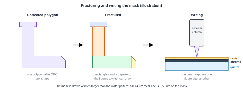
The data volume grows at each step. Hierarchy is the first casualty: the multiplier's GDSII stores each standard cell once and references it, but the flattened top cell has 42,667 mcon cuts and 27,221 licon cuts. OPC then gives every edge its own correction, so identical cells in different neighbourhoods no longer share data, and fracturing breaks every corrected polygon into many figures. For a large chip at an advanced node, the mask data of one critical layer is far larger than the whole GDSII of the design.
Modern scanners reduce the mask image four times, so the mask pattern is four times larger than the wafer pattern. A minimum met1 width of 0.14 um on the wafer is 0.56 um on the mask.
Inspection, Repair and the Pellicle
A defect on a mask is printed on every die of every wafer exposed with it, so masks are inspected far more strictly than wafers. Inspection tools compare the mask with its own data, or one die with an identical die on the same mask. Small defects are repaired, for example by removing extra chrome or depositing material into a missing spot with a focused beam.
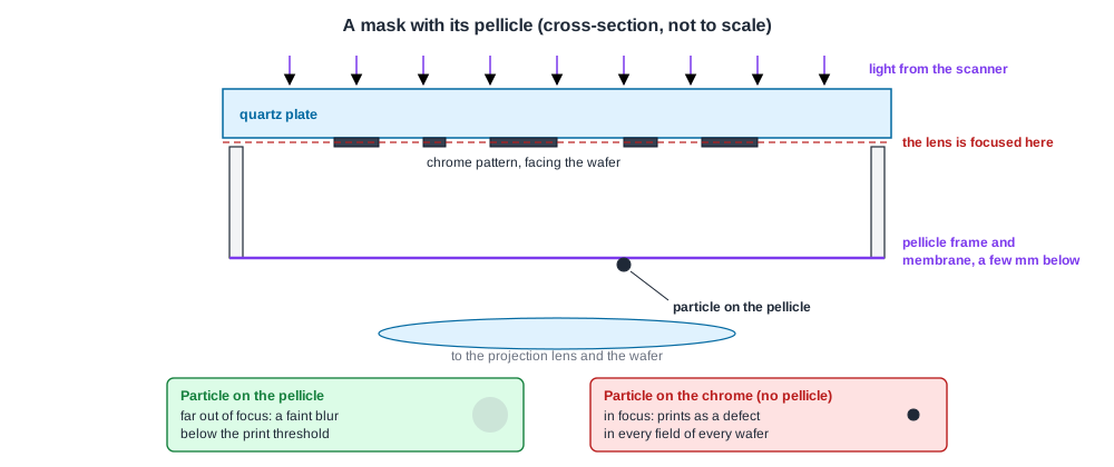
The finished mask gets a pellicle: a thin transparent membrane on a frame a few millimetres above the pattern. A particle that lands on the pellicle is out of focus and does not print. Masks are then stored and handled in clean cassettes and re-inspected regularly, because a mask is used for many thousands of exposures.
Quick Check
Q: Why can a single particle on a mask be worse than a single particle on a wafer?
Show Answer
A particle on a wafer can kill at most the dies it lands on, once. A particle on the mask pattern is printed in every exposure field, on every wafer, until it is found. That is why masks are inspected strictly and protected with a pellicle, which holds particles out of focus.
What Masks Cost
A mask set is a one-time cost for each design revision, and it is dominated by the critical layers: active, poly, contact and the lowest metals, which need the finest writing, the most OPC and the strictest inspection. A critical mask costs in the vicinity of $100,000 at 65 nm, a full set above $1 million, roughly doubling with each node, and the metal masks can be cheaper than the lower layers because their pitch is looser.
That cost explains several habits seen earlier in this tutorial. Spare cells and metal-only ECOs, as in ECOs After Routing, exist so that a fix needs new metal masks only. Shared wafers exist so that small designs do not pay for a whole set. And sign-off is strict because every respin buys masks again.
Running It in ChipVerify Lab
Run Place and Route on the multiplier and download the GDSII. Open it in KLayout and list the layers: compare them with the drawn column of the table above, and look for a mask without a drawn layer, such as the nitride seal or the tip implants. Then flatten the top cell and count the shapes on mcon (67/44) and licon1 (66/44); the counts show how much larger a mask layer's data is than the hierarchical file suggests.
Common Mistakes
Mistake #1: Assuming each drawn layer is one mask
Masks are derived from drawn layers, some from combinations of them, and some masks have no drawn layer at all.
Mistake #2: Expecting the printed shape to match the mask
The mask is corrected so that the print matches the layout. Mask and print differ on purpose.
Mistake #3: Forgetting that a mask defect repeats
One mask defect is a defect in every exposure field. Mask inspection and the pellicle exist for this reason.
Practice Exercise
Challenge: Scaling to the Mask
A scanner with four times reduction exposes a field of 26 x 33 mm on the wafer. How large is the pattern area on the mask? The minimum met1 spacing in sky130 is 0.14 um on the wafer: what is it on the mask? Standard mask plates are about 152 mm (6 inches) square; does the field fit?
Hint
Multiply every wafer dimension by four.
Solution
The pattern is 104 x 132 mm on the mask, and the 0.14 um spacing becomes 0.56 um. A 104 x 132 mm pattern fits on a 152 mm plate with room for the frame, alignment marks and the pellicle frame around it.
Open the ready-made example in the lab, synthesize it and run Place and Route.
Summary
- Masks are process layers derived from the drawn layers; the sky130 list marks 34 masks as used, with names such as FOM, P1M, LICM1 and MM1.
- Some masks have no drawn layer; the foundry creates them by CAD or they belong to unused options.
- OPC and other resolution enhancements change the mask so that the print matches the layout.
- Fracturing turns flattened, corrected polygons into rectangles and trapezoids for e-beam or laser writing.
- Masks are inspected, repaired and covered with a pellicle, because a mask defect repeats in every field.
- Critical layers dominate mask cost, which drives metal-only ECOs, shared wafers and strict sign-off.