
Clock gating switches off the clock to a group of flip-flops whenever they do not need to change. It is the most effective dynamic power technique in digital design, because the clock is the one signal that toggles every cycle. For physical design, a clock gate is a cell in the middle of the clock tree: CTS has to build a tree to the gates, a tree behind each gate, and keep the latencies of gated and ungated flip-flops balanced. This article compares a 32 x 16-bit register file built with enable flip-flops against the same register file with one clock gate per register.
8 min read | Intermediate
What You'll Learn
- Explain how an integrated clock gating cell works
- Compare enable flip-flops with clock gating in area and power
- Describe how CTS handles clock gates
- Recognise the placement problem behind long gated clock trees
Two Ways to Hold a Register
A register that is written only sometimes must keep its value in the other cycles. There are two ways:
- Enable flip-flops: each flip-flop has a multiplexer that feeds its own output back when the enable is low. The clock still toggles every cycle on every flip-flop. In sky130 hd, synthesis maps this to
edfxtp_1, a flip-flop with a DE (data enable) pin, 30 um2 against 20 um2 for a plaindfxtp_1. - Clock gating: plain flip-flops, and one clock gating cell per register that passes the clock only in cycles when the register is written.
An AND gate on the clock would glitch if the enable changed while the clock is high. The integrated clock gating cell (ICG) avoids that with a latch: sky130_fd_sc_hd__dlclkp_1 captures GATE while CLK is low and outputs GCLK = CLK AND the latched GATE. The enable can change at any time during the low phase without producing a partial pulse.
The Two Register Files
The enable version is plain RTL, and synthesis picks enable flip-flops by itself:
always @(posedge clk) begin
  for (i = 0; i < 32; i = i + 1) begin
    if (we && waddr == i)
      mem[i] <= wdata;
  end
end
The gated version instantiates one ICG per register. The (* blackbox *) declaration tells synthesis that the cell exists in the library, so it keeps the instance as it is:
(* blackbox *)
module sky130_fd_sc_hd__dlclkp_1 (
  output GCLK,
  input  CLK,
  input  GATE
);
endmodule

genvar g;
generate
  for (g = 0; g < 32; g = g + 1) begin : row
    sky130_fd_sc_hd__dlclkp_1 icg (
      .GCLK (gclk[g]),
      .CLK  (clk),
      .GATE (we && waddr == g)
    );

    always @(posedge gclk[g]) begin
      mem[g] <= wdata;
    end
  end
endgenerate
Commercial synthesis tools insert clock gates automatically from the enable RTL; the lab's Yosys flow does not, so the cell is instantiated by hand here.
What CTS Does With Clock Gates
TritonCTS recognises the clock gates and splits the work:
[INFO CTS-0011]  Clock net "clk" for macros has 32 sinks.
[INFO CTS-0011]  Clock net "clk_regs" for registers has 16 sinks.
[INFO CTS-0010]  Clock net "gclk\[9\]" has 16 sinks.
...
[INFO CTS-0008] TritonCTS found 34 clock nets.
...
[INFO CTS-0033] Balancing latency for clock clk
[INFO CTS-0036]  inserted 3 delay buffers
- The 32 clock gates are sinks of the main tree.
- The 16 output flip-flops that are not gated get a tree of their own,
clk_regs. - Each of the 32 gated clocks gets its own small tree to its 16 flip-flops: 34 clock nets in total.
- Flip-flops behind a gate see the gate's delay plus their own tree. To match them, CTS inserted 3 delay buffers in front of the ungated
clk_regstree.
The balancing shows in a hold path between the two kinds of flip-flop:
   0.12    0.12 ^ clkbuf_0_clk/X (sky130_fd_sc_hd__clkbuf_8)
   0.18    0.30 ^ clkbuf_2_2__f_clk/X (sky130_fd_sc_hd__clkbuf_8)
   0.15    0.45 ^ row[27].icg/GCLK (sky130_fd_sc_hd__dlclkp_1)
   0.13    0.58 ^ clkbuf_0_gclk[27]/X (sky130_fd_sc_hd__clkbuf_8)
   0.14    0.72 ^ clkbuf_1_0__f_gclk[27]/X (sky130_fd_sc_hd__clkbuf_8)
   0.00    0.72 ^ _1151_/CLK (sky130_fd_sc_hd__dfxtp_1)
...
   0.09    0.09 ^ delaybuf_0_clk/X (sky130_fd_sc_hd__clkbuf_8)
   0.10    0.20 ^ delaybuf_1_clk/X (sky130_fd_sc_hd__clkbuf_8)
   0.10    0.30 ^ delaybuf_2_clk/X (sky130_fd_sc_hd__clkbuf_8)
   0.10    0.40 ^ clkbuf_regs_0_clk/X (sky130_fd_sc_hd__clkbuf_8)
   0.11    0.52 ^ clkbuf_0_clk_regs/X (sky130_fd_sc_hd__clkbuf_8)
   0.13    0.65 ^ clkbuf_1_0__f_clk_regs/X (sky130_fd_sc_hd__clkbuf_8)
   0.00    0.65 ^ _1599_/CLK (sky130_fd_sc_hd__dfxtp_1)
The gated flip-flop is reached after 0.72 ns, through two buffers, the clock gate and two more buffers. The output flip-flop is reached after 0.65 ns, through the three delay buffers and its own tree. The balancing was not perfect: the skew between them is 0.07 ns. After routing, the clock latencies of the whole design range from 0.69 to 0.92 ns, a skew of 0.23 ns, compared with 0.03 ns for the register file without gates.
Quick Check
Q: Why does CTS have to add delay to the ungated flip-flops, rather than leaving their clock as fast as possible?
Show Answer
Data flows between gated and ungated flip-flops. If the ungated ones were clocked much earlier, the skew on those paths would be large, hurting setup in one direction and hold in the other. Matching the latencies keeps the skew small.
The Gated Clock Trees
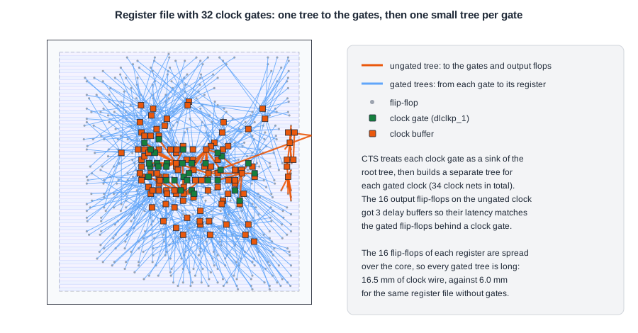
The picture shows a problem that the numbers alone hide. The clock gates sit together near the middle, but the 16 flip-flops of each register are spread all over the core. The placer put each flip-flop next to the read multiplexer logic for its bit, not next to the other bits of its register, because the placement did not know that the flip-flops of one register share a gated clock. Every gated tree therefore spans most of the block.
The Comparison
| Register file, 32 x 16 bits | Enable flip-flops | One clock gate per register |
|---|---|---|
| Storage flip-flops | 512 edfxtp_1 | 512 dfxtp_1 + 32 dlclkp_1 |
| Design area | 23,752 um2 | 18,568 um2 (-22 %) |
| Clock buffers from CTS | 81 | 104 + 3 delay buffers |
| Routed clock wire | 5.87 mm | 17.08 mm |
| Clock skew after routing | 0.03 ns | 0.23 ns |
| Clock network power | 2.55 mW | 0.53 mW |
| Flip-flop (sequential) power | 2.48 mW | 0.16 mW |
| Total power | 5.16 mW | 0.81 mW |
Area went down by 22 %, because a plain flip-flop plus a shared clock gate is smaller than an enable flip-flop. The clock tree got worse in every physical measure: more buffers, almost three times the clock wire and about eight times the skew.
The power dropped by a factor of six anyway. The power numbers use the tool's default activity on the inputs, under which we is high half the time and the write address is random, so each register is written only in a small fraction of cycles. Behind a closed gate, the flip-flops' clock pins and the gated tree do not toggle at all. The real saving depends on how often each register is actually written; with a vector-based activity file from simulation it could be smaller or larger, but the direction is the same.
Quick Check
Q: The gated design has almost three times as much clock wire. Why is its clock power still much lower?
Show Answer
Power depends on how often a wire switches, not only on its capacitance. Most of the extra wire is in the gated trees, which switch only in the cycles when their register is written. The main tree, which switches every cycle, drives 48 sinks instead of 528.
Better Placement for Gated Clocks
Long gated trees cost clock power in the cycles when the gate is open, and they make skew harder to control. The usual remedies:
- Gate at a coarser level, one gate for a group of registers that are placed together, or a hierarchy of gates.
- Clone the clock gate, one copy near each cluster of its flip-flops, so each copy drives a short local tree.
- Clock-gating-aware placement, which pulls flip-flops of the same gated clock closer together. Commercial flows do this, along with gate cloning and merging during CTS.
Running It in ChipVerify Lab
Write the two register files in the lab, synthesize them and run Place and Route on both. Each needs more than the free tier's five minutes; with PRO, the plain one took about five and a half minutes and the gated one about nine. Compare the cell area, the number of clock nets TritonCTS reports, the final skew and the power report. In the gated version, find the clock gates in the layout and see where the flip-flops of one register ended up.
Common Mistakes
Mistake #1: Gating the clock with a plain AND gate
If the enable changes while the clock is high, the output produces a short glitch that can clock the flip-flops. Use the library's latch-based ICG cell.
Mistake #2: Judging clock gating by the clock tree's quality
The gated tree here had more buffers, more wire and more skew, and the design still used six times less power. Judge it by power with realistic activity, and check timing separately.
Mistake #3: Forgetting the enable timing of the clock gate
The ICG's GATE input has a setup check against the clock, like a flip-flop. Its enable logic must arrive before the clock's rising edge, with the gate's own clock latency taken into account.
Practice Exercise
Challenge: Where the Area Went
An edfxtp_1 is 30.0 um2, a dfxtp_1 20.0 um2 and a dlclkp_1 17.5 um2. Estimate the area saved by replacing 512 enable flip-flops with plain flip-flops and 32 clock gates. Compare with the measured difference of 5,184 um2.
Hint
Saving = 512 x (30.0 - 20.0) - 32 x 17.5.
Solution
5,120 - 560 = 4,560 um2. Most of the rest of the measured 5,184 um2 is buffering: repair_design inserted 99 buffers in the enable version, mostly on the heavily loaded enable and data nets, and only 13 in the gated version.
Open the ready-made example in the lab, synthesize it and run Place and Route.
Summary
- A latch-based ICG passes the clock only when its enable is set, without glitches.
- TritonCTS builds a tree to the gates and one behind each gate, and adds delay buffers to balance ungated flip-flops.
- On the register file, clock gating cut area by 22 % and power by a factor of six at default activity.
- The gated trees were long, 16.45 mm against 5.95 mm, because each register's flip-flops were spread over the core.
- Gate cloning, coarser gating and gating-aware placement shorten gated trees.
