
In a flip-chip design, the chip connects to its package through solder bumps spread over its whole top surface, not through wires bonded to a ring of pads at the edge. The chip is flipped face down onto the package substrate, and the bumps melt to form the connections. This removes the perimeter limit on the number of connections, shortens every supply path, and lets power enter right above the logic that uses it. It also adds new physical design tasks: the bump map, the redistribution layer that routes from I/O cells to bumps, and the assignment of every signal and supply to a bump. This article covers them, with counts calculated for real die sizes and the commands OpenROAD provides.
8 min read | Intermediate
What You'll Learn
- Compare the connection counts of peripheral pads and area bump arrays
- Describe a bump map and how supplies and signals are assigned to bumps
- Explain the redistribution layer and how it is routed
- Read the OpenROAD commands for bump arrays and RDL routing
From the Edge to the Whole Area
Flip-chip, also called controlled collapse chip connection (C4), was developed by IBM in the 1960s. Solder balls are attached to pads on the top metal in a final step called wafer bumping, and the chip is flipped and heated so the balls melt onto the package. Bumps can be placed on a pitch of 150 um or less, giving thousands of connections; one Xeon processor, for example, has 13,164 bumps, most of them for power and ground, bringing 120 A onto the chip.
The gain in connection count comes from geometry. A ring of pads grows with the perimeter, an array of bumps with the area:
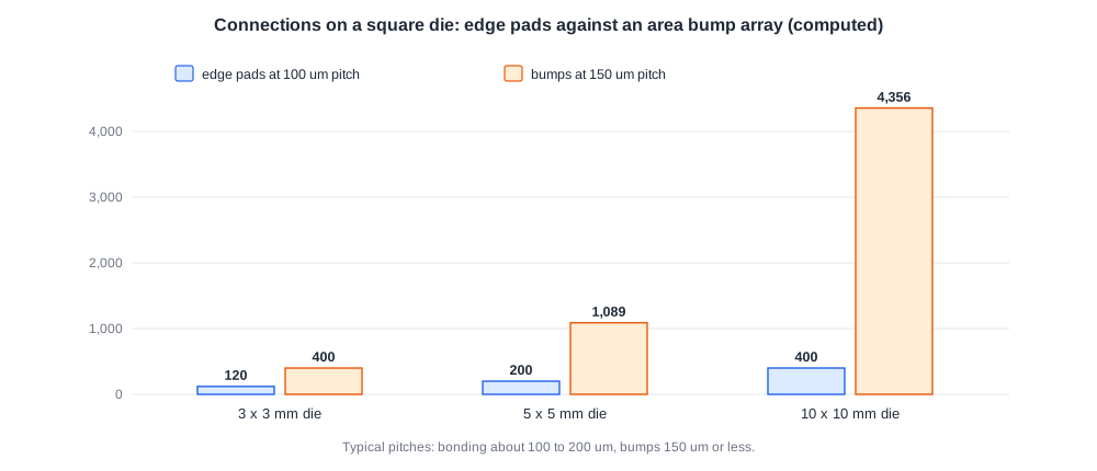
| Die side | Edge pads at 100 um pitch | Bumps at 150 um pitch | Bumps at 500 um pitch |
|---|---|---|---|
| 3 mm | 120 | 400 | 36 |
| 5 mm | 200 | 1,089 | 100 |
| 10 mm | 400 | 4,356 | 400 |
The edge column uses 100 um, the lower end of the usual wire-bond pad pitch; the bump columns count full rows and columns of the array. At a fine pitch the array wins by a large factor, and the factor grows with the die. At a coarse pitch, such as the 0.5 mm of a wafer-level package that is soldered directly to a board, a small die has fewer bump sites than edge pads.
Caravel is an example of the coarse case. Its documentation describes a wafer-level chip-scale package with a 6 x 10 ball array at 0.5 mm pitch, 60 balls, for a padframe of 44 GPIO cells and 18 supply pads. Its 3,588 x 5,188 um die has room for 7 x 10 sites at that pitch.
Quick Check
Q: Doubling the side of a die doubles its number of edge pads. What happens to the number of bumps at a fixed pitch?
Show Answer
It roughly quadruples, because the bump array fills the area, which grows with the square of the side. The table shows it: from 5 mm to 10 mm, edge pads go from 200 to 400 and bumps at 150 um from 1,089 to 4,356.
The Bump Map
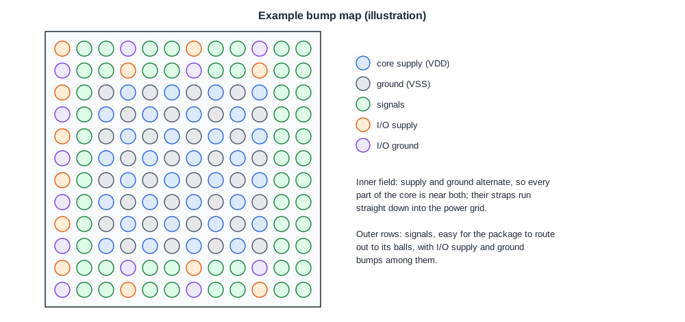
Every bump is assigned a net. A typical map, like the illustration, follows a few rules:
- Supply and ground fill the centre. Bumps over the core alternate between supply and ground in a regular pattern, so every point of the core is close to both, and their straps on the top metal connect straight down into the power grid.
- Signals use the outer rows. The package substrate has to route every signal from its bump out to a ball; bumps near the edge escape easily, inner ones need more substrate layers.
- I/O supplies sit among the signals, for the same reasons as the interleaved supply pads of Power and Ground Pads: How Many and Where.
- Differential pairs and buses get neighbouring bumps, in order.
The map is a contract with the package designer, who must be able to route the substrate from these bumps to the package balls. It is usually negotiated back and forth, as Chip-Package Co-Design describes.
Bumps over the core change the power analysis too. The supply no longer enters at the edge and travels inward; it enters at every bump. That is the model the lab's IR drop analysis uses by default, with a regular bump pattern over the block, in Power Sign-Off: IR Drop and EM.
Area I/O and the Redistribution Layer
The I/O cells do not have to move to the centre when the chip goes flip-chip. Many designs keep a peripheral ring of I/O cells and connect each one to its bump with a wire on a redistribution layer (RDL): one or more thick metal layers above the normal stack, used only for these connections. The sky130 mask list includes such an option: a copper redistribution layer with its polymer layers, used for the wafer-level package described in Dicing and Packaging.
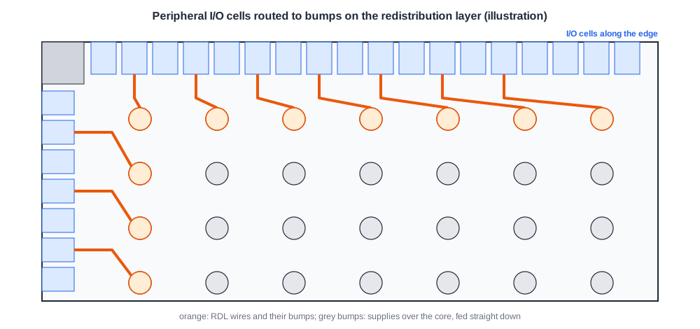
Alternatively, an area-I/O design places the I/O cells anywhere in the core, each under or next to its bump, which shortens the connection further but breaks the pad ring into islands, each needing its own supplies and ESD paths.
RDL routing has its own character. The layer is thick and its wires wide, there are few layers, often just one, and every wire must reach a bump without crossing another. Routers allow 45-degree segments to squeeze wires between bumps, and they try to keep routes straight.
Bumps and RDL in OpenROAD
OpenROAD's pad module includes commands for the whole flow; the examples below are from its documentation. They are not available in the lab at the time of writing.
# a 14 x 14 array of bump instances, 200 um pitch, starting at (200, 200)
make_io_bump_array -bump BUMP -origin "200 200" -rows 14 -columns 14 -pitch "200 200"

# assign nets to bumps
assign_io_bump -net DVSS BUMP_6_4
assign_io_bump -net DVDD BUMP_7_3
assign_io_bump -net p_ddr_addr_9_o BUMP_6_0

# route the redistribution layer from the I/O pins to the bumps
# (RDL_LAYER: the name of the redistribution layer in the technology LEF)
rdl_route -layer RDL_LAYER -allow45 {p_ddr_addr_9_o}
make_io_bump_arraycreates the bumps as instances named by row and column.assign_io_bumpconnects a net to a bump;-terminalchooses which pin of a multi-pin I/O cell it should reach.rdl_routeroutes the chosen nets on the RDL layer, with options for width, spacing, a turn penalty that favours straight routes, and-allow45.place_io_terminalscreates top-level terminals on the I/O cells' pad pins, so the chip's ports land on the pads.
Quick Check
Q: Why are supply bumps over the core usually connected straight down into the top power straps instead of through the RDL?
Show Answer
A bump directly above a strap needs only a via stack, which is short and low in resistance and inductance. Routing it through the RDL to the edge and back in would add length, resistance and inductance and use RDL area needed for signals. The point of supply bumps over the core is to feed the grid where the current is drawn.
The Costs of Flip-Chip
- Bumping and substrate cost. Wafer bumping is an extra process, and a substrate that escapes hundreds of bumps needs several layers.
- Test and debug. The top-level metal is no longer accessible for probing during debug, since the chip faces the package.
- Mechanical stress. Silicon and substrate expand differently with temperature; underfill spreads the stress, and the floorplan follows rules about large metal and sensitive circuits under bumps.
- A bump plan in the floorplan. The top metal layers must leave room for bump pads at the bump pitch, which constrains the power straps and macro placement from the start.
Running It in ChipVerify Lab
At the time of writing, the lab has no bump or RDL steps. Its IR drop analysis does model supply bumps: the report prints the bump pitch it assumed, and the power grid it analyses is the one built in Building a PDN in OpenROAD. The connection counts in this article are calculations; the Caravel figures are from its documentation and layout files.
Common Mistakes
Mistake #1: Putting signal bumps in the middle of the array
Inner signals are hard to escape in the package. Keep signals in the outer rows and supplies inside.
Mistake #2: Planning the power grid without the bump pitch
Straps that do not line up with the supply bumps need extra metal to reach them. Align the top straps to the bump pattern.
Mistake #3: Assuming flip-chip means no pad ring
Peripheral I/O cells with RDL routing are common; they still need the ring's supplies and ESD paths.
Practice Exercise
Challenge: Signals Versus Supplies
A 6 x 6 mm die uses bumps at 150 um pitch. Half of all bumps go to supply and ground, as in many high-performance chips. How many signal bumps remain, and how does that compare with a wire-bond ring at 100 um pitch on the same die?
Hint
6,000 / 150 = 40 bumps per side.
Solution
The array has 40 x 40 = 1,600 bumps; half for supplies leaves 800 for signals. A wire-bond ring at 100 um holds 4 x 60 = 240 pads, of which supplies would also take a share. Even after giving half the bumps to power, the flip-chip die has more than three times as many signal connections as the whole wire-bond ring.
Summary
- Flip-chip connects the die face down through solder bumps over its whole area.
- Bump count grows with area: a 10 mm die holds 4,356 bumps at 150 um pitch against 400 edge pads at 100 um.
- Bump maps put supply and ground over the core and signals in the outer rows.
- A redistribution layer routes peripheral I/O cells to their bumps; area I/O places the cells under the bumps.
- OpenROAD provides make_io_bump_array, assign_io_bump, rdl_route and place_io_terminals.
