
All the current a chip uses enters through its supply pads or bumps and leaves through its ground pads. Each of those connections has inductance and resistance, so the number of supply pads, and where they sit, decides how much the supply bounces when outputs switch or the core wakes up. Most high-performance chips devote about half their pins to power and ground. This article shows where that number comes from: the ground bounce of switching outputs, the current steps of the core, the separation of noisy and quiet supplies, and the placement rules that follow.
8 min read | Intermediate
What You'll Learn
- Calculate ground bounce from simultaneously switching outputs
- Estimate how many ground pads an output group needs
- Explain why I/O and core supplies are kept separate
- Place supply pads to keep noise and IR drop low
Inductance in the Supply Path
A bond wire is not just a resistor. Its inductance is about 1 nH per millimetre, while a flip-chip solder bump is on the order of 100 pH. A changing current through an inductance creates a voltage across it:
V = L x dI/dt
When the current through a ground pad rises quickly, the chip's internal ground rises above the board's ground by this voltage. Every signal referenced to that ground shifts with it. This is ground bounce, and its counterpart on the supply side is supply droop. Inductors in parallel divide their inductance, so more pads mean less bounce.
Simultaneously Switching Outputs
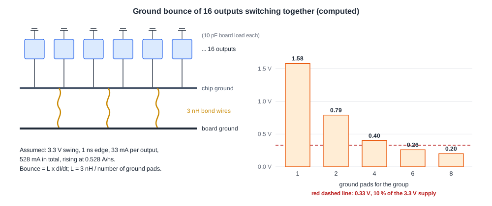
Outputs are the biggest source of fast current steps. Take a 16-bit bus switching together, with these assumptions:
- each output drives 10 pF on the board, with a 3.3 V swing and a 1 ns edge;
- the ground connections are bond wires 3 mm long, so 3 nH each;
- the current rises from zero to its full value within one edge time.
Each output then carries C x dV/dt = 10 pF x 3.3 V / 1 ns = 33 mA during the edge, 528 mA for all sixteen. That current rises in about 1 ns, so dI/dt is 0.528 A/ns:
| Ground pads for the group | Inductance | Ground bounce |
|---|---|---|
| 1 | 3 nH | 1.58 V |
| 2 | 1.5 nH | 0.79 V |
| 4 | 0.75 nH | 0.40 V |
| 6 | 0.5 nH | 0.26 V |
| 8 | 0.375 nH | 0.20 V |
With one ground pad, the internal ground jumps by almost half the I/O supply, which could flip the inputs of other pads. To keep the bounce under 10 % of 3.3 V, the group needs five ground pads, roughly one for every three outputs. The same calculation with 100 pH flip-chip bumps gives 0.05 V for a single bump, one of the reasons flip-chip packages handle wide, fast buses better.
The calculation also shows the other levers. Doubling the edge time to 2 ns halves the current per output and spreads it over twice the time, cutting dI/dt by four: 0.40 V with a single pad. That is what the slow mode of the sky130 GPIO cell, from I/O Cells: Drivers, Receivers and Level Shifting, is for. Lower loads, lower swings and outputs that do not all switch at once help in the same way.
Quick Check
Q: A designer halves the board load of every output and also switches the bus in two groups of eight, half a nanosecond apart. By how much does the ground bounce change, roughly?
Show Answer
Halving the load halves each output's current, and therefore dI/dt. Splitting into two groups whose edges barely overlap halves the peak current again. Together the bounce falls to about a quarter. The exact value depends on how much the two groups' edges overlap.
Core Current Steps
The core produces current steps too, when a block wakes up, a clock gate opens, or a burst of activity starts. Consider a chip whose current jumps from 20 A to 60 A in one 1 ns cycle; with 20 pH of supply inductance the noise would be 0.8 V without on-chip bypass capacitance.
A small chip shows the same effect at a smaller scale. If the core current steps from 0.1 A to 0.5 A in 5 ns through 3 nH bond wires, the droop is 3 nH x 0.4 A / 5 ns = 0.24 V with one supply pad, 0.12 V with two, 0.06 V with four. Decoupling capacitance on the die, from Tap Cells, Endcaps, Latch-Up and Decaps, supplies the first nanoseconds of such a step locally, and the supply pads and package capacitors supply the rest.
Dirty and Quiet Supplies
Because output switching is so noisy, it is good practice to separate the supply that feeds the output drivers from the core supply. The I/O drivers get their own pads and buses, often called the "dirty" supply, and the core and any analog circuits get their own "quiet" supplies. The separation is essential when the I/O runs at a different voltage than the core, and useful even when it does not.
The sky130 I/O cells reflect this: they have separate I/O supplies (VDDIO, VSSIO), quiet I/O references (VDDIO_Q, VSSIO_Q), analog supplies (VDDA, VSSA) and core supplies (VCCD, VSSD). Caravel brings in each of these through its own pads: vddio at 3.3 V for the I/O and ESD, vccd at 1.8 V for the management core, vdda at 3.3 V for analog, and separate 1.8 V and 3.3 V supplies for each of the two user areas.
How Many Pads, and Where
The pad count for each supply comes from several limits, and the largest one wins:
- Noise. The ground bounce and droop calculations above, for each output group and for the core.
- Current per pad. Each pad, bond wire or bump has a maximum current, from electromigration in its metal and heating in the wire. The I/O library and the package documentation give the values.
- IR drop. The resistance from the pad through the ring bus and the core grid to the farthest cell, analysed as in IR Drop: Static and Dynamic with the real pad positions as sources.
- ESD. Clamped supply pads must be close enough to every signal pad, as in ESD Protection for Physical Designers.
Placement rules follow from the same physics:
- Interleave supply and ground pads with output groups, so each group's current returns through nearby pads. Wide buses are interdigitated with many power and ground pins.
- Put core supply pads near the blocks that draw the most current.
- Place a supply pad and its ground pad next to each other, so the current loop through the package is small.
- Spread pads around all sides, which helps IR drop, ESD and noise at once.
- Keep analog supply pads away from fast digital outputs.
Quick Check
Q: A core-limited chip has 12 unused pad slots. What is a good use for them?
Show Answer
Extra supply and ground pads, placed among the output groups and near the busiest blocks. They lower the supply inductance and IR drop and add ESD clamps at no area cost, because the die size is set by the core.
Caravel's Supply Pads
Caravel's padframe, read in Building the Pad Ring, has 18 clamped supply pads for 44 GPIO cells, about one supply pad for every 2.4 signal pads, spread over all four sides. In its package, several ground pads share balls, and the documentation's pinout lists the grounds vssio, vssa and vssd together on four balls. Package decisions like this one are the subject of Chip-Package Co-Design.
Running It in ChipVerify Lab
The lab's IR drop analysis, described in Power Sign-Off: IR Drop and EM, assumes supply bumps over the block or feeds the grid from its strap pins with PRO. It does not model pad inductance at the time of writing. The noise numbers in this article are calculations with the stated assumptions and typical inductance values.
Common Mistakes
Mistake #1: Counting supply pads from average current only
Average current sets IR drop and electromigration, but ground bounce depends on how fast the current changes. Check both.
Mistake #2: Sharing the core supply with the output drivers
Output switching noise then reaches every core cell. Give the I/O its own supply and ground.
Mistake #3: Putting all ground pads at one end of a bus
Outputs far from the ground pads see a long, inductive return path. Interleave ground pads with the outputs.
Practice Exercise
Challenge: A 32-Bit Bus
A 32-bit output bus drives 5 pF per pin with a 1.8 V swing and a 2 ns edge. Ground bond wires are 2 mm long at 1 nH/mm. How many ground pads keep the bounce below 0.18 V?
Hint
Find the current per output, the total dI/dt, then the allowed inductance.
Solution
Each output: 5 pF x 1.8 V / 2 ns = 4.5 mA; all 32: 144 mA, rising in 2 ns, so 0.072 A/ns. The allowed inductance is 0.18 V / 0.072 A/ns = 2.5 nH. One wire is 2 nH, so a single pad gives 0.144 V and already meets the limit. Two pads would add margin for the bounce of other groups sharing the ground.
Summary
- Supply connections have inductance, about 1 nH/mm for bond wires and 100 pH for bumps, so fast current changes cause ground bounce and droop.
- Sixteen 10 pF outputs switching in 1 ns through one 3 nH ground wire bounce the ground by 1.58 V; five ground pads bring it under 0.33 V.
- Slower edges, lower loads and staggered switching reduce dI/dt.
- I/O drivers get their own dirty supply, separate from the quiet core and analog supplies.
- Pad count is the largest of the noise, current, IR drop and ESD limits; pads are interleaved with outputs and spread around the ring.
