
Electrostatic discharge (ESD) is the sudden current that flows when a charged person, machine or chip touches a conductor. A few kilovolts on a fingertip is harmless to a person but can puncture a gate oxide a few nanometres thick, so every pad of a chip needs a protection path that carries the discharge safely to a supply. The protection devices come with the I/O library, but whether they work depends on the layout around them: the buses they discharge into, the clamps between supplies, and the resistance of the whole path. This article explains the models, the protection network, and what the physical designer has to get right.
8 min read | Intermediate
What You'll Learn
- Describe the human body model and the charged device model
- Trace the discharge path through diodes, buses and supply clamps
- Calculate why bus resistance matters during a discharge
- List the layout rules and checks for ESD
Why Chips Need Protection
An input pad connects, through the receiver, to transistor gates. The oxide breakdown voltage was 40 to 100 V for older thick oxides and is now 5 V or less for thin ones. A discharge can also cause punchthrough, where the source and drain depletion regions meet and a large current flows through an off transistor until it overheats, and it can trigger latch-up.
The idea of protection is to give the discharge an easier path than the gates: devices that turn on well before any oxide is in danger and carry the current to a robust supply network.
The Test Models
ESD robustness is measured by zapping each pin with a standard circuit and finding the highest voltage the chip survives. Two models matter most:
- Human body model (HBM). A 100 pF capacitor, charged to the test voltage, discharges into the pin through 1,500 ohms, representing a person touching the pin.
- Charged device model (CDM). The chip itself is charged, for example by sliding along a surface during manufacturing, and discharges when one pin touches a grounded conductor. The current is short and very fast, and it flows out from inside the chip, so it stresses different paths than HBM.
The HBM peak current follows from Ohm's law across the 1,500 ohm resistor, because the protection network's own resistance is small:
| HBM level | Peak current |
|---|---|
| 2 kV | 1.33 A |
| 4 kV | 2.67 A |
| 8 kV | 5.33 A |
| 15 kV | 10.0 A |
Typical targets are plus or minus 15 kV for parts a user can touch through a cable, such as serial port transceivers, and 2 to 4 kV for parts inside an enclosed system that only see ESD during assembly. Amperes of current through a chip's metal is far beyond anything in normal operation, which is why ESD shapes the layout.
Quick Check
Q: Why does a CDM event need protection close to the circuits it protects, even when every pad has good HBM protection?
Show Answer
In CDM the charge is stored on the chip itself, spread over its supply networks and substrate, and it rushes out through the pin that touches ground. The fast current can flow through internal paths, for example from a core supply through a gate connected to an I/O signal, without passing the pad's primary protection. Local clamps and resistors next to the receiving gates limit the voltage there.
The Protection Network
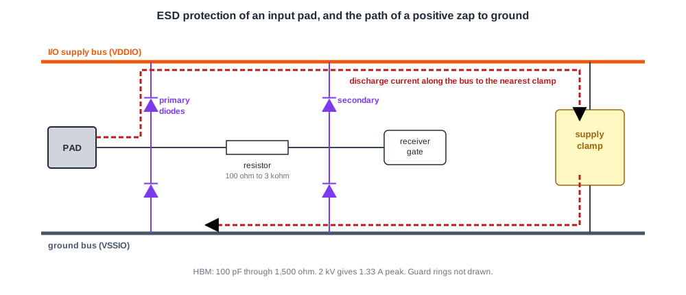
A typical input protection circuit has:
- Primary diodes from the pad to the supply and from ground to the pad. They turn on when the pad goes more than about 0.7 V above the supply or below ground, and a good protection diode has an on-resistance of about 1 ohm.
- A series resistor, anywhere from 100 ohms to 3 kilohms, limits the current reaching the inner circuit.
- Secondary diodes, smaller, next to the receiver, limit the voltage the gates see.
- Guard rings around all these devices, so their large currents do not inject carriers into the substrate and trigger latch-up.
The diodes alone are not enough. A positive zap from the pad to ground first turns on the diode to the I/O supply, and the current must then get from the supply bus to ground. A supply clamp, a large transistor between the supply and ground that turns on during a fast voltage rise, completes the path. In sky130, the supply pads include these clamps: the library's power pads are described as having an "ESD high-voltage clamp" for the 3.3 V supplies or an "ESD low-voltage clamp" for the 1.8 V ones, and Caravel uses the clamped versions for all 18 of its supply pads.
The Bus Is Part of the Path
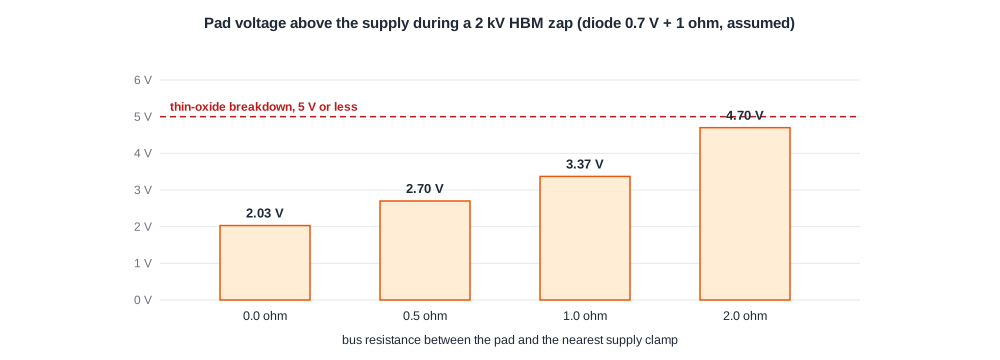
The discharge path runs through the pad ring's supply buses, from the pad that is zapped to the nearest clamp. During a 2 kV HBM zap, 1.33 A flows. With a diode drop of 0.7 V and 1 ohm of diode resistance, the pad rises to about 2.0 V above the supply even with a perfect bus. Every ohm of bus resistance between the pad and the clamp adds 1.33 V:
| Bus resistance to the clamp | Pad voltage during the zap |
|---|---|
| 0 ohm | 2.03 V |
| 0.5 ohm | 2.70 V |
| 1 ohm | 3.37 V |
| 2 ohm | 4.70 V |
These numbers are an illustration with the stated diode values, but the trend is real: a long, narrow path to the nearest clamp can bring a thin oxide close to its breakdown voltage. That is why the ring buses are wide, why they must be continuous, and why supply pads with clamps are spread around the ring instead of grouped in one place.
Quick Check
Q: A chip has all its supply pads, and therefore all its clamps, on one side of the ring. Which pads are least protected, and why?
Show Answer
The pads on the opposite side. Their discharge current must travel half way around the ring through the bus to reach a clamp, so the bus resistance, and the voltage the pad reaches during a zap, is largest for them. Spreading clamped supply pads around the ring shortens every path.
Several Supply Domains
A zap can enter on a pin of one domain while the other pin touches ground in another domain. The discharge must then cross between grounds that are deliberately kept separate, for example a quiet analog ground and a noisy digital one. Libraries provide back-to-back diodes between such grounds: they conduct only during an ESD event, when the grounds differ by more than a diode drop, and leave the grounds isolated in normal operation. Caravel splits and joins its ring buses with dedicated slices so that each domain's segment still has a discharge path.
Signals that cross between domains inside the core are a classic CDM weak point. A gate in one domain driven by a long wire from another can see the full difference between the two supplies during an event. ESD rule decks check for these crossings and ask for local protection or a resistor next to the receiving gate.
What the Physical Designer Checks
- Every pad has a protected cell. No bare pads, except where the library provides a specific unprotected analog cell and the design accepts the risk.
- The ring is continuous. Every supply bus closes around the ring, or ends at a domain split the ESD plan intends.
- Clamps are close enough. The library specifies the maximum bus resistance or distance between any pad and its clamps.
- Discharge paths are wide. Connections from pads to protection devices, and from devices to buses, use the widths the library requires, often many times the electromigration width, because ESD currents are amperes.
- Latch-up rules near the I/O: guard rings and spacing between I/O devices and core logic.
- Cross-domain checks for gates driven from another domain.
Commercial flows run these checks with programmable electrical rule checkers that trace the paths from every pad and compute their resistance. In open flows, the I/O library's documented rules and careful ring construction carry most of the burden.
Running It in ChipVerify Lab
At the time of writing, the lab's flow has no I/O cells or ESD devices, so these checks cannot be run there. The pad types in this article come from the sky130 I/O library and the Caravel padframe.
Common Mistakes
Mistake #1: Trusting the I/O cell alone
The cell's diodes only move the current to a bus. The bus and the supply clamps complete the path.
Mistake #2: Grouping all supply pads together
Clamps far from a pad leave it weakly protected. Spread clamped supply pads around the ring.
Mistake #3: Ignoring cross-domain signals
Signals between domains need checking for CDM stress at the receiving gate.
Practice Exercise
Challenge: Bus Width for ESD
A pad must stay below 3.0 V above the supply during a 2 kV HBM zap. The protection diode drops 0.7 V and has 1 ohm of resistance. The bus to the nearest clamp is 1,500 um long, with a sheet resistance of 0.03 ohm per square. How wide must the bus be?
Hint
Find the allowed bus resistance first, then the number of squares.
Solution
The current is 2,000 / 1,500 = 1.33 A. The diode takes 0.7 + 1.33 x 1 = 2.03 V, leaving 0.97 V, so the bus may have 0.97 / 1.33 = 0.73 ohm. At 0.03 ohm per square that is 24 squares, so the bus must be at least 1,500 / 24 = 62 um wide.
Summary
- ESD can destroy thin gate oxides; every pad needs a protection path to a supply.
- HBM uses 100 pF through 1,500 ohms, so a 2 kV zap carries 1.33 A; CDM discharges the chip itself, fast and from the inside.
- Primary diodes, a series resistor, secondary diodes and supply clamps form the protection network.
- The ring bus is part of the discharge path; its resistance adds directly to the pad voltage.
- Spread clamped supply pads, keep buses continuous and wide, protect cross-domain gates and follow the latch-up rules.
