
Dicing cuts the finished wafer into individual dies along the scribe lanes, and packaging gives each good die the connections, protection and heat path it needs to sit on a circuit board. The package is not an afterthought for physical design: whether the die is wire-bonded at its edge or flipped onto solder bumps over its whole area decides where the pads go, how power enters the chip, and how the I/O ring and the power grid are planned. This article covers thinning and dicing, the two ways of connecting a die, the common package types, and what each one asks of the layout.
7 min read | Intermediate
What You'll Learn
- Describe wafer thinning and the main dicing methods
- Explain the role of the scribe lane and the seal ring
- Compare wire bonding and flip-chip, and the packages built on each
- Connect the package choice to pads, bumps and the power grid
Thinning and Dicing
A finished 300 mm wafer is a little under 1 mm thick, much thicker than a package needs. Before dicing, the wafer is mounted face down on a protective tape and ground thinner from the back, often to a few hundred micrometres, and further for stacked or very thin packages. Thinning also helps heat leave the die.
The thinned wafer is mounted on a dicing tape stretched over a metal frame, and cut along the scribe lanes:
- Blade dicing. A thin diamond saw cuts through the wafer. It is the classic method; the cut (the kerf) and the chipping beside it need a scribe lane wide enough to contain them.
- Laser dicing. A laser ablates a groove, sometimes followed by a blade, which avoids mechanical stress on fragile low-k dielectrics.
- Stealth dicing. A laser focused inside the silicon creates a weakened layer along the lane, and stretching the tape splits the dies apart with almost no kerf, which allows narrower lanes.
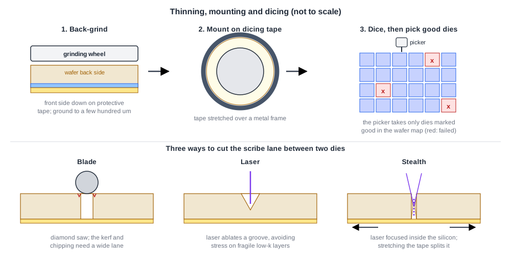
The dies stay on the tape in their wafer positions, so the die-picking machine can use the wafer map from sort, described in Who Does What After Tapeout, and pick only the good ones.
The Scribe Lane and the Seal Ring
The scribe lane holds the foundry's test structures and alignment marks, all of which the saw destroys. The edge of each die is protected by the seal ring, a continuous wall of every metal and via layer, tied into the passivation, that stops cracks from the saw and moisture from creeping in sideways through the dielectric stack.
The sky130 layer tables show that the seal ring is not just a few lines of metal: there are marker layers for the seal ring area, for a "deadzone" around it used for metal stress relief checks, and for critical corners and sides where stress rules apply. Large metal shapes near the die corners are restricted because the corners take the highest stress when the package cools after assembly.
Quick Check
Q: A team wants to save area by placing a small calibration circuit in the scribe lane next to its die. What happens to it?
Show Answer
It is cut away during dicing, so it is available only at wafer sort, never in the packaged part. Structures needed after packaging must sit inside the seal ring, in the die itself.
Wire Bond or Flip-Chip
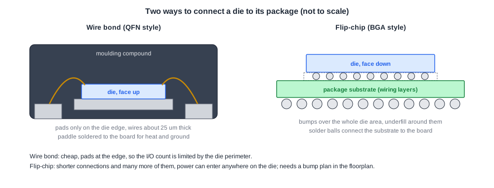
Wire bonding glues the die face up onto the package and connects each pad to the package with a thin wire. Gold wires are about 25 um thick, and the pad pitch is limited by the bonding machine to about 100 to 200 um, so the pads sit in a ring around the die edge, the pad frame. Copper wire is now common for cost, and fine-pitch bonding reaches below that range, but the principle is the same: the I/O count is limited by the perimeter. A chip with many I/Os and little logic can become pad-limited, its size set by the pad ring rather than the core.
Flip-chip puts solder bumps or copper pillars on pads in the top metal over the whole die area, flips the die face down and melts the bumps onto a package substrate. Underfill epoxy fills the gap and spreads the mechanical stress. The connections are shorter, with far less inductance than bond wires, and there can be thousands of them. Power and ground can enter anywhere on the die, which makes the on-die power grid much more effective.
Common Package Types
| Package | Die connection | Board connection | Typical use |
|---|---|---|---|
| QFN, QFP | wire bond | leads or pads on the package edge, exposed paddle underneath | small and medium I/O counts, low cost |
| Wire-bond BGA | wire bond to a substrate | solder ball array | more I/O than leaded packages |
| Flip-chip BGA | bumps to a substrate | solder ball array | processors, high-speed and high-power chips |
| WLCSP | none: built on the wafer | solder balls on the die itself | small dies in phones and wearables |
| 2.5D and 3D | bumps to an interposer or another die | substrate and balls | chiplets, memory stacks |
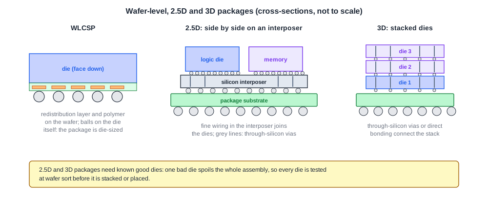
A wafer-level chip-scale package (WLCSP) is the smallest: the package is the die plus a redistribution layer that moves the pads to a ball grid, a protective layer and the balls, all processed on the whole wafer before dicing. The sky130 PDK documentation includes WLCSP rules from two packaging providers, and its mask list has the masks for this option: a copper redistribution layer (CU1M), a polymer layer (PBO) and a second polyimide (PMM2).
2.5D packages place several dies side by side on a silicon interposer with very fine wiring; 3D stacks dies on top of each other, connected by through-silicon vias or direct bonding. Both need known good dies, because one bad die spoils the whole stack.
What the Package Asks of the Layout
- Pads or bumps. A wire-bond chip needs an I/O ring with pads, ESD protection and power pads at the edge, as listed in GDSII Out and Tapeout. A flip-chip needs a bump map, decided at floorplanning, with power and ground bumps spread over the core.
- Power entry. With edge pads, current enters at the periphery and the IR drop is worst in the centre; with bumps it enters all over. This is why IR Drop: Static and Dynamic depends on where the supply connections are assumed.
- Pin order. The order of signals around the die must suit the package and the board; reversing it later means a new floorplan.
- Stress. Keep-out rules near corners and under bumps protect fragile dielectrics during assembly and thermal cycling.
Quick Check
Q: Why does a flip-chip package usually show lower IR drop in the centre of a large die than a wire-bonded one?
Show Answer
With wire bonding, all supply current enters through pads at the edge and must cross the whole on-die grid to reach the centre. With flip-chip, power bumps sit over the core, so every region has a supply connection close by and the current paths through the grid are short.
Running It in ChipVerify Lab
Run Place and Route on the multiplier and open the IR drop section of the report. The lab assumes a grid of supply bumps over the block, 70 um bumps at a 140 um pitch, because the block has no power pins of its own: in effect, a flip-chip connection. Compare the worst drop with the drop near a bump; then think about how much larger it would be if all current entered from one edge.
Common Mistakes
Mistake #1: Choosing the package after the floorplan
Pads, bumps, pin order and power entry are floorplan decisions. Decide the package first.
Mistake #2: Ignoring a pad-limited die
If the I/O count sets the die size, shrinking the core saves nothing. Count pads at the start.
Mistake #3: Treating the seal ring as optional
Without it, cracks and moisture enter from the sawn edge and the die fails over time.
Practice Exercise
Challenge: Pads or Bumps
A die is 5 x 5 mm. How many wire-bond pads fit around its edge at a 100 um pitch, ignoring the corners? How many flip-chip bumps fit over its area at a 200 um pitch? If the core needs 400 I/O and power connections, which option works?
Hint
Pads: perimeter divided by pitch. Bumps: a square grid of (side / pitch) per row.
Solution
Pads: 4 x 5,000 / 100 = 200, fewer in practice because the corners are lost. Bumps: (5,000 / 200)2 = 25 x 25 = 625. Only the flip-chip option provides 400 connections; with wire bonding the die would have to grow, becoming pad-limited.
Open the ready-made example in the lab, synthesize it and run Place and Route.
Summary
- Wafers are thinned from the back, mounted on tape and diced by blade, laser or stealth dicing along the scribe lanes.
- The seal ring, with its own keep-out and stress rules, protects the die edge after sawing.
- Wire bonding connects edge pads face up; flip-chip connects bumps over the whole die face down.
- Package types range from leaded and QFN packages to flip-chip BGAs, wafer-level packages and 2.5D or 3D stacks.
- The package decides pads or bumps, power entry, pin order and stress rules, so it must be chosen before the floorplan.
