
Stopping the clock of an idle block saves power, and the usual way is to put a gate in the clock path. But a gate in a clock path is dangerous: if the enable signal changes at the wrong moment, the gated clock gets a short pulse, called a glitch, that can corrupt every flip-flop behind it. STA protects against this with clock gating checks. This article explains the risk, shows the two checks that STA adds on its own, and compares a correct and an incorrect design with real numbers.
9 min read | Intermediate
What You'll Learn
- Explain how an enable that changes at the wrong time creates a glitch on a gated clock
- Describe the clock gating setup and hold checks of an AND gate
- Read a clock gating report and find the violation
- Say how the enable has to be generated to pass the checks
The Risk
A clock gate is an ordinary gate in the clock path with one input for the clock and one for an enable. With an AND gate, the clock goes through when the enable is 1 and the output stays at 0 when the enable is 0:
module sta_gate (input clk, a, d, output q);
  reg en, r;
  always @(posedge clk)
    en <= a;                         // enable flip-flop
  wire gclk = clk & en;              // the clock gate
  always @(posedge gclk)
    r <= d;                          // flip-flop on the gated clock
  assign q = r;
endmodule
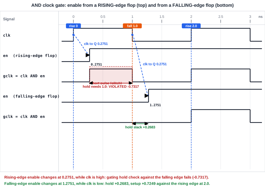
Look at the gate. When the clock is high, the output follows the enable. If the enable changes from 0 to 1 while the clock is high, the output rises in the middle of the clock pulse, and the pulse is shorter than it should be. If the enable changes from 1 to 0 while the clock is high, the output falls early. Either way, the gated clock has a pulse that is cut short, and a flip-flop may react to it, or not. To avoid this, an AND gate needs its enable to change only while the clock is low.
The Two Checks
STA recognizes a gate that has a clock on one input and data on the other, and it adds a clock gating check automatically. For an AND gate, it has two parts, both made against the clock edges at the gate:
- The clock gating setup check: the enable must be stable before the clock rises. The capture edge is the rising edge of the clock.
- The clock gating hold check: the enable must not change until after the clock falls. The capture edge is the falling edge of the clock.
In other words, the enable may change only in the time when the clock is low. For an OR gate the rule is the opposite: the enable may change only while the clock is high.
Quick Check
Q: For an AND clock gate, when may the enable change?
Show Answer
Only while the clock is low, between the falling edge and the next rising edge. If it changes while the clock is high, the gated clock gets a glitch.
A Violation
In the design above, the enable comes from a flip-flop that is clocked on the rising edge. It changes right after the clock rises, just when the clock is high, and the check shows it. The report puts these checks in a separate path group, gated clock:
Startpoint: _2_ (rising edge-triggered flip-flop clocked by clk)
Endpoint: _0_ (rising clock gating-check end-point clocked by clk)
Path Group: gated clock
Path Type: min

   0.0000    0.0000 ^ _2_/CLK (sky130_fd_sc_hd__dfxtp_1)
   0.2683    0.2683 v _2_/Q (sky130_fd_sc_hd__dfxtp_1)
   0.0000    0.2683 v _0_/B (sky130_fd_sc_hd__and2_0)
             0.2683   data arrival time

   1.0000    1.0000   clock clk (fall edge)
   0.0000    1.0000 v _0_/A (sky130_fd_sc_hd__and2_0)
   0.0000    1.0000   clock gating hold time
             1.0000   data required time
            -0.7317   slack (VIOLATED)
The endpoint is the gate input B, marked as a clock gating check end point. The enable changes at 0.2683 ns, but it must not change before the clock falls at 1.0 ns. The violation is -0.7317 ns. The setup check is met, with a slack of 1.7249 ns, because the enable arrives long before the next rising edge at 2.0 ns. This is a typical pattern: the setup check looks fine and the hold check shows the real mistake.
The Fix: Change the Enable While the Clock Is Low
The enable must come from something that changes while the clock is low. The simplest way is a flip-flop that is clocked on the falling edge. A real design usually uses a latch that is open while the clock is low, a cell called an integrated clock gate, which also solves the setup problem. With a falling-edge flip-flop, the enable changes at 1.0 + 0.2751 = 1.2751 ns:
always @(negedge clk)
  en <= a;
| Check | Arrival (ns) | Required (ns) | Slack (ns) |
|---|---|---|---|
| Gating setup (rising edge at 2.0) | 1.2751 | 2.0000 | 0.7249 |
| Gating hold (falling edge at 1.0) | 1.2683 | 1.0000 | 0.2683 |
Both checks now pass. The enable changes in the time window between the falling edge at 1.0 ns and the next rising edge at 2.0 ns, and it has 0.2683 ns of margin at the start and 0.7249 ns at the end. Compare this with the first design: the enable changed at 0.2683 ns, 0.7317 ns before the clock fell.
The same flip-flop now has a path from the enable flip-flop to a rising-edge flip-flop, and from an input to the falling-edge flip-flop. These are half-cycle paths, with a launch on the falling edge and a capture on the rising edge. They have only half of the clock period. Half-Cycle Paths shows how STA handles them.
Quick Check
Q: For an OR clock gate the rule is the reverse: the enable may change only while the clock is high. Which kind of flip-flop is a natural source for its enable?
Show Answer
A rising-edge flip-flop. Its output changes shortly after the rising edge, while the clock is high, which is the safe time for an OR gate, as long as it settles before the clock falls.
Common Mistakes
Mistake #1: Gating a clock with a signal from a rising-edge flip-flop
The enable changes while the clock is high, which breaks the gating hold check of an AND gate. Use a latch-based or falling-edge enable.
Mistake #2: Trusting a clean setup check
For an AND gate, the gating setup check is easy to meet. The violation is in the gating hold check, so look at the gated clock path group for both types.
Practice Exercise
Challenge: Find and Fix the Gating Violation
Paste the sta_gate design into the lab, with a 2.0 ns clock, input delays of 0.4 ns on a and d, and an output delay of 0.4 ns on q. Run STA and look at the group gated clock. Find the hold slack. Then change the enable flip-flop to always @(negedge clk) and run again.
Hint
The launch edge of the enable moves from the rising edge to the falling edge of the clock, which is half a period later.
Solution
With the rising-edge flip-flop, the gating hold slack is -0.7317 ns (violated), and the gating setup slack is 1.7249 ns. With the falling-edge flip-flop, the hold slack becomes +0.2683 ns and the setup slack 0.7249 ns. Both are met. The enable data now arrives half a period later, which is what the AND gate needs. Check the numbers in your run: the cell names can differ, but the change of exactly half the period holds.
Open the ready-made example in the lab, run synthesis, and then run STA. Editing constraints.sdc and re-running only STA, and choosing another library or corner, are PRO features.
Summary
- A gate in the clock path creates a glitch if the enable changes while the clock input of the gate is active.
- STA adds clock gating checks automatically and reports them in a separate path group.
- For an AND gate the setup check is against the rising edge and the hold check is against the falling edge of the clock.
- The enable of an AND gate may change only while the clock is low.
- An enable from a rising-edge flip-flop violates the gating hold check, here by -0.7317 ns.
- A falling-edge flip-flop, or a latch-based clock gate cell, fixes the problem.
