
The library tables ask for one number for the load of a cell output: a capacitance. A real net with wire resistance is more than a single capacitor, so which number should the tool use? The answer is the effective capacitance, a value that is smaller than the total capacitance of the net. This article explains why, how the tool finds it, and what it changes in a timing report.
Think of a driver that fills a big bucket through a narrow hose. If the driver is quick, it is finished before the far part of the bucket has received much water, so it behaves as if the bucket were smaller. That smaller, effective size is what this article is about.
7 min read | Intermediate
What You'll Learn
- Explain why a driver does not see the full capacitance of a resistive net
- Describe the pi model that represents a net for delay calculation
- Define the effective capacitance and say how it is used in the delay lookup
- Predict when the effective capacitance is close to the total and when it is much smaller
The Driver Does Not See All the Capacitance
Take a driver that is connected to a wire with a resistor in the middle. The capacitor near the driver is charged immediately. The capacitor behind the resistor is charged only through that resistor, and it takes some time. If the output of the driver changes quickly, it may have finished its transition before much charge has reached the far capacitor.
From the point of view of the driver, the far capacitor is partly hidden behind the resistance. This is called resistive shielding. The driver acts as if its load were smaller than the sum of all the capacitors.
A delay table is built from simulations with a pure capacitor as load. To use the table for a resistive net, the tool needs one capacitor that makes the driver behave in the same way as the real net does. That value is the effective capacitance, written Ceff.
The Pi Model
To find Ceff, the tool first reduces the whole RC tree, however large, to a small circuit that looks the same from the driver. The usual reduction is the pi model, so called because its shape looks like the Greek letter. It has three parts: a capacitor C1 near the driver, a resistor Rpi, and a capacitor C2 behind the resistor.
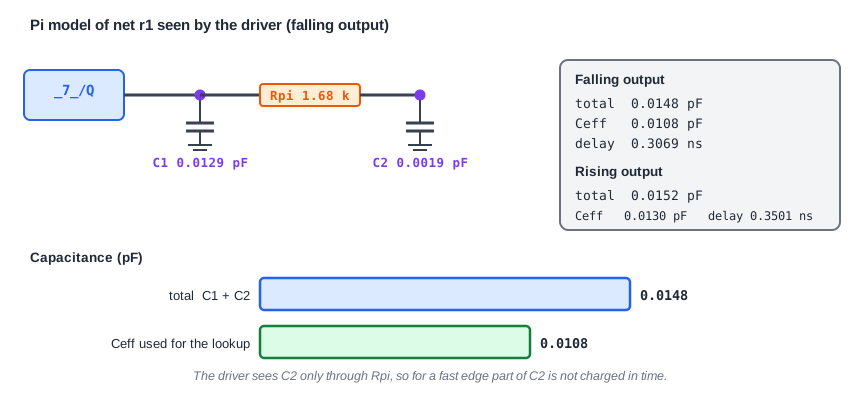
For the net r1 of the demo circuit, the tool creates this model for the falling output of the flip-flop _7_. You can see it in the delay calculation report of the tool:
Arc type: Reg Clk to Q
CLK ^ -> Q v
Pi model C2=0.0019 Rpi=1.6839 C1=0.0129, Ceff=0.0108
C1 and C2 add up to 0.0148 pF, the total capacitance of the net. The effective capacitance of 0.0108 pF is smaller by about a quarter. The tool looks up the clock-to-Q delay in the table with a load of 0.0108 pF, and gets 0.3069 ns.
How the Tool Finds Ceff
The value of Ceff is not a fixed property of the net. It depends on the driver and on the edge. The tool starts with a guess, such as the total capacitance, and finds the output slew from the library table. It then calculates how much charge the pi model takes until the output has made half of its transition. It adjusts Ceff, looks up the table again, and repeats this a few times until the value settles.
You do not need to do this by hand. What matters is the result: the table lookup uses Ceff, and the pins and nets in the report show the load that was used.
When Ceff Is Close to the Total
The size of the shielding depends on how the transition of the driver compares with the time constant of the wire. For a fast driver edge and a resistive wire, a lot of capacitance is hidden and Ceff is small. For a slow edge, there is time to charge everything, and Ceff approaches the total.
The same net shows both cases. For the rising output of _7_, the library slew is 0.1325 ns, which is more than twice the 0.0610 ns of the falling output, and the result is:
CLK ^ -> Q ^
Pi model C2=0.0020 Rpi=1.7026 C1=0.0132, Ceff=0.0130
Delay = 0.3501
The total capacitance is 0.0152 pF, and Ceff of 0.0130 pF is close to it. The slower edge lets the far capacitor take part. The rising and the falling output of the same pin therefore use different load values, and that is one more reason why a report shows rising and falling delays separately.
Why It Matters
Using the total capacitance instead of Ceff would give a larger load, and the delay table would give a larger delay. The result is pessimistic, and the error can be large when the wire resistance is high.
A lumped capacitor with the same total value shows the difference. When the load of r1 is replaced by 0.009 pF of lumped wire capacitance, the clock-to-Q delay becomes 0.3206 ns, compared with 0.3069 ns for the real net with the same total. A lumped model makes the cell slower, because it does not know about the shielding. It also loses the net delay, which is why the two effects need to be modelled together.
Common Mistakes
Mistake #1: Thinking Ceff is the same as the total capacitance
The total capacitance is a property of the net. The effective capacitance depends on the net, the driver and the transition. It is always at most the total for a net with resistance, and it is different for the rising and the falling output.
Mistake #2: Looking up the table with the capacitance that the report prints for the net
The load shown in the path report is the total capacitance of the net. The delay of the driver was looked up with Ceff, which is smaller. A hand calculation with the printed load gives a slightly larger delay than the tool.
Quick Check: Why is the effective capacitance of a fast driver smaller than that of a slow driver on the same net?
A fast edge is finished before the capacitance behind the resistor is charged, so part of that capacitance is hidden. A slow edge lasts long enough to charge it, so the driver sees almost all of it.
Practice Exercise
Challenge: Compare the Two Edges
This is a pencil and paper exercise, because the lab does not read parasitic files. The net r1 has the following pi models:
| Output edge | C1 (pF) | C2 (pF) | Ceff (pF) |
|---|---|---|---|
| Falling | 0.0129 | 0.0019 | 0.0108 |
| Rising | 0.0132 | 0.0020 | 0.0130 |
Find the total capacitance for each edge. Then calculate how large a part of the total the driver sees, as a percentage, and say which edge has more shielding.
Hint
The total is C1 + C2. The part the driver sees is Ceff divided by the total.
Solution
The totals are 0.0129 + 0.0019 = 0.0148 pF for the falling edge and 0.0132 + 0.0020 = 0.0152 pF for the rising edge. The driver sees 0.0108 / 0.0148 = 73 percent of the falling total and 0.0130 / 0.0152 = 86 percent of the rising total. The falling edge has more shielding, because the driver edge is faster there.
Summary
- A resistive net hides part of its capacitance from the driver, which is called resistive shielding.
- The net is reduced to a pi model with two capacitors, C1 and C2, and a resistor between them.
- The effective capacitance, Ceff, is the single capacitor that makes the driver behave as with the real net.
- The cell delay is looked up in the table with Ceff and not with the total capacitance.
- Ceff depends on the driver and the edge: a fast edge gives more shielding, a slow edge less.
- A lumped capacitor with the total value overestimates the cell delay and misses the net delay.
