
Think of a chip as a map of roads. A timing path is one route on that map: it starts where a signal begins its journey and ends where the signal is caught and stored. Static timing analysis finds every such route and checks that the signal gets there in time, so you need to know exactly where a route begins and ends. This article defines the start and end points and the four kinds of route that appear in every timing report.
6 min read | Intermediate
What You'll Learn
- Identify the startpoints and endpoints of a timing path
- Classify a path as input to register, register to register, register to output or input to output
- Compute a path delay as the sum of cell and net delays
- Explain why setup uses the longest path and hold uses the shortest
Paths, Startpoints and Endpoints
Every path has a startpoint, an endpoint, and some logic and wires in between. The logic is called combinational logic: gates such as AND, OR and XOR that have no memory and just react to their inputs. A signal starts its journey in one of two ways: it comes in from outside the chip, or a flip-flop sends it when the clock ticks. So the startpoints are:
- Input ports of the design
- Clock pins of sequential cells, such as the
CLKpin of a flip-flop
A signal ends its journey when it leaves the chip or when a flip-flop catches it. So the endpoints are:
- Output ports of the design
- Data input pins of sequential cells, such as the
Dpin of a flip-flop
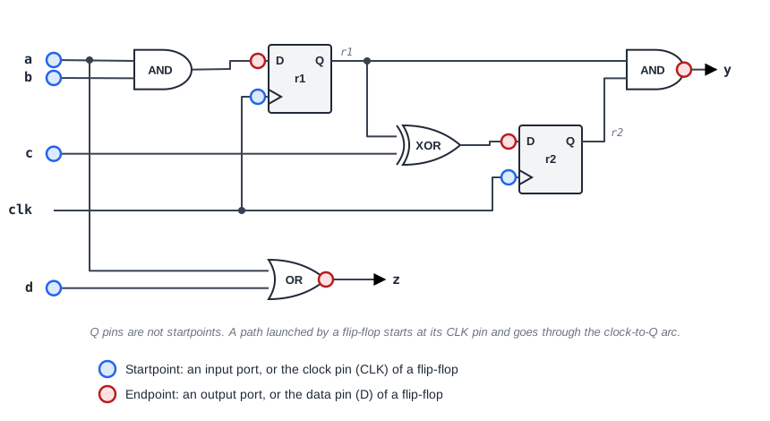
Note that the Q pin of a flip-flop is not a startpoint. Data is launched by the clock edge arriving at the CLK pin, and the path then travels through the clock-to-Q delay of the flip-flop before it reaches Q. That is why a timing report for a register path begins at CLK.
The Four Path Types
Two kinds of startpoint and two kinds of endpoint give four kinds of path. Each has a short name that you will see in every report. The highlighted paths below are in the circuit used throughout this series.
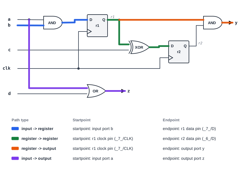
- Input to register: data enters the chip and is captured by a flip-flop. The external logic that drives the input is described by an input delay.
- Register to register: one flip-flop launches data and another captures it. This is the core of a synchronous design. The launching flip-flop is called the launch flop and the capturing one the capture flop.
- Register to output: data leaves the chip. The logic that receives it is described by an output delay.
- Input to output: a purely combinational path with no flip-flop in it. It has to fit in one clock period together with both the input delay and the output delay.
Here are the setup numbers for the four paths from the sta_demo design, with a 2.0 ns clock and 0.4 ns input and output delays:
| Path type | Startpoint | Endpoint | Data arrival (ns) | Setup slack (ns) |
|---|---|---|---|---|
| Input to register | b | _7_/D | 0.5201 | 1.3639 |
| Register to register | _7_/CLK | _6_/D | 0.4323 | 1.4502 |
| Register to output | _7_/CLK | y | 0.3956 | 1.2044 |
| Input to output | a | z | 0.5674 | 1.0326 |
Several paths can end at the same endpoint. The register _6_ is reached from both c and _7_/CLK. A summary reports the worst path to each endpoint, and for _6_/D that is the one starting at c, with a slack of 1.3650.
A Path Delay Is a Sum
The delay of a path is the sum of the delays of the cells and nets along it. For the register-to-register path, the flip-flop contributes its clock-to-Q delay and the XOR gate contributes its cell delay:
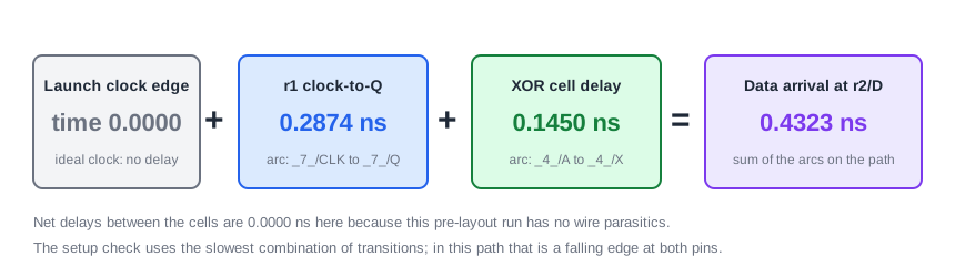
             0.0000    0.0000    0.0000 ^ _7_/CLK (sky130_fd_sc_hd__dfxtp_1)
   0.0058    0.0401    0.2874    0.2874 v _7_/Q (sky130_fd_sc_hd__dfxtp_1)
             0.0401    0.0000    0.2874 v _4_/A (sky130_fd_sc_hd__xor2_1)
   0.0017    0.0367    0.1450    0.4323 v _4_/X (sky130_fd_sc_hd__xor2_1)
             0.0367    0.0000    0.4323 v _6_/D (sky130_fd_sc_hd__dfxtp_1)
                                 0.4323   data arrival time
The Delay column holds the delay added by each step and the Time column is the running total. The rows ending in /A and /D are nets, and their delay is 0.0000 because this analysis has no wire parasitics. The chapter on Liberty libraries later in this series shows how cell delays are looked up.
Longest and Shortest Paths
Between two points there is often more than one path, because logic can reconverge. The path with the largest total delay is the max path, also called the late path. The one with the smallest is the min path, or early path. Longest and shortest refer to the accumulated delay, not to the number of cells.
Setup and hold look at opposite ends. A setup check asks whether data can arrive too late, so it uses the max path. A hold check asks whether data can arrive too early, so it uses the min path. In the same register-to-register path, the setup arrival is 0.4323 ns while the hold arrival is 0.3657 ns, because the fastest transitions through the flip-flop and the XOR are different ones from the slowest.
STA also sorts paths into path groups, by the clock of the capturing element. Every path in our demo belongs to the group clk, which is why each report header shows Path Group: clk.
Common Mistakes
Mistake #1: Leaving the clock-to-Q delay out of a register path
The data does not appear at Q at the clock edge. It appears after the clock-to-Q delay, which is 0.2874 ns in this path. Leave it out and you underestimate every register path.
Mistake #2: Assuming the longest path has the most gates
A path with two slow, heavily loaded cells can be longer in delay than a path with five fast ones. STA ranks paths by accumulated delay, so the critical path is not always the deepest logic cone.
Quick Check: What are the startpoint and endpoint of the path from input port a to the data pin of r1?
The startpoint is the input port a and the endpoint is the D pin of r1. It is an input-to-register path.
Practice Exercise
Challenge: Spend the Budget on One Output
Start from the sta_demo constraints with a 2.0 ns period. Change only the output delay of y to 1.0 ns by adding this line after the existing set_output_delay line, then re-run STA:
set_output_delay 1.0 -clock clk [get_ports y]
Predict the new setup slack of y and say which other endpoints should change.
Open the ready-made example in the lab, run synthesis, and then run STA. Editing constraints.sdc and re-running only STA, and choosing another library or corner, are PRO features.
Hint
The required time of an output path is the clock period minus the output delay. The arrival time of the register-to-output path depends only on the cells.
Solution
The required time of y becomes 2.0 - 1.0 = 1.0 ns, while the arrival time stays 0.3956 ns, so the setup slack falls from 1.2044 to 0.6044 ns. The other endpoints do not change, because the new delay is attached only to y. The hold slack on y changes too, because the same output delay is used with the opposite sign for the hold check, which Setup and Hold: The Two Fundamental Checks explains.
Summary
- Paths start at input ports or flip-flop clock pins and end at output ports or flip-flop data pins.
- The four path types are input to register, register to register, register to output and input to output.
- A path delay is the sum of the cell and net delays along it, and a register path includes the clock-to-Q delay.
- The max (late) path decides setup and the min (early) path decides hold.
- Longest means largest delay, not most cells.
- Paths are grouped by the clock of the capturing element, and reports show the worst path per endpoint.
