
Most paths in a design start or end at a flip-flop. A combinational feedthrough path does neither. The signal enters at an input port, goes through gates only, and leaves at an output port. There is no flip-flop to stop it, so the whole path has to fit inside a single clock period, together with the delays of the outside world. This article shows how to constrain such a path, why it is often the one that limits the clock, and what happens when the constraints are incomplete.
7 min read | Intermediate
What You'll Learn
- Recognize a combinational feedthrough path and say how it is constrained
- Calculate the time budget of an input-to-output path
- Calculate the smallest clock period that such a path allows
- Explain what happens to the path if one of the two delays is missing
The Path
In the demo circuit, the output z is the result of an OR gate of the two inputs a and d:
assign z = a | d; // input -> output, no flip-flop
The data goes from the port a straight to the port z. It is not launched by a flip-flop of this chip, and it is not captured by one. STA still needs a launch edge and a capture edge, so it uses the clock of the input delay and the clock of the output delay. For a path with both constraints, it works like any other path:
- The arrival time is the input delay plus the delay of the gate.
- The required time is the clock period minus the output delay.
The Budget
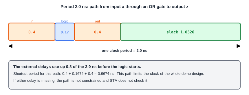
Everything that happens on this path must fit in one period. The outside device before the chip uses the input delay, the gate takes its delay, and the outside device after the chip needs the output delay. What is left is the slack:
Slack = Tperiod - input delay - gate delay - output delay
      = 2.0 - 0.4 - 0.1674 - 0.4 = 1.0326 ns
The report of this path, which is the worst setup path of the demo design, has no flip-flop in it:
Startpoint: a (input port clocked by clk)
Endpoint: z (output port clocked by clk)
Path Type: max

   0.0000    0.0000   clock clk (rise edge)
   0.4000    0.4000 v input external delay
   0.0000    0.4000 v a (in)
   0.1674    0.5674 v _2_/X (sky130_fd_sc_hd__or2_0)
   0.0000    0.5674 v z (out)
             0.5674   data arrival time

   2.0000    2.0000   clock clk (rise edge)
  -0.4000    1.6000   output external delay
             1.6000   data required time
             1.0326   slack (MET)
The Smallest Period
Because the path does not include any flip-flop delay or setup time, the smallest period is the sum of the three delays: 0.4 + 0.1674 + 0.4 = 0.9674 ns. Run the demo design at this period and the slack is 0.0000 ns. At 0.97 ns the slack is +0.0026 ns (met), and at 0.96 ns it is -0.0074 ns (violated). This is the path that limits the clock of the whole demo design, even though the longest path between flip-flops is much shorter. A path with an external delay on both ends often has the smallest slack in a design.
Hold
The hold check of a feedthrough path asks that the new data does not arrive before the outside device has finished with the old data. Both ends use the same clock edge. In the demo circuit, the earliest data from the input d arrives at 0.4 + 0.0488 = 0.4488 ns, and the requirement at the output is minus the output delay, -0.4 ns. The hold slack is 0.4488 - (-0.4) = 0.8488 ns. The period is not in this equation, as for every hold check.
When One of the Delays Is Missing
If the input delay is missing, STA has no launch clock for the path, and if the output delay is missing, it has no capture clock. In both cases the path is not constrained and is not checked. In the article about validating constraints, the missing output delay on z makes the worst setup slack look better, 1.2044 ns instead of 1.0326 ns, with no warning in the report.
Feedthrough paths are easy to forget because they do not appear in the list of flip-flops. Check them by name: every input must have an input delay and every output must have an output delay, including the ones that only connect through gates.
Different Clocks at the Two Ends
The input delay and the output delay do not have to use the same clock. If they use two different clocks, such as two virtual clocks, STA picks the launch and capture edges as in the article about clock groups. When the two devices run from the same clock, it is simplest to use the same virtual clock or the clock of the chip at both ends.
Common Mistakes
Mistake #1: Giving the feedthrough path the full period
A designer who sees a 2.0 ns clock may think the gate has 2.0 ns. But the delays of the outside world use part of it, and with 0.4 ns on each side, the gate has at most 1.2 ns.
Mistake #2: Leaving the output delay out because there is no flip-flop
The output delay is needed whether or not a flip-flop sits in the path. Without it, the path ends at an output that has no timing requirement, and nothing is checked.
Quick Check: A feedthrough path has an input delay of 0.5 ns, a logic delay of 0.3 ns and an output delay of 0.6 ns. What is the smallest clock period?
0.5 + 0.3 + 0.6 = 1.4 ns.
Practice Exercise
Challenge: Find the Limit of the Clock
Use the sta_demo design with the basic constraints. Predict the smallest period at which the path from a to z meets setup. Then run STA with a period of 0.97 ns and with 0.96 ns. Finally, change the input delay of all inputs to 0.6 ns and predict the new smallest period.
Open the ready-made example in the lab, run synthesis, and then run STA. Editing constraints.sdc and re-running only STA, and choosing another library or corner, are PRO features.
Hint
The smallest period is the input delay plus the gate delay plus the output delay. The gate delay is 0.1674 ns.
Solution
With input and output delays of 0.4 ns the smallest period is 0.9674 ns. At 0.97 ns the slack is +0.0026 ns and at 0.96 ns it is -0.0074 ns. With an input delay of 0.6 ns, the period must be at least 0.6 + 0.1674 + 0.4 = 1.1674 ns. Other paths, for example the register paths, will have different limits, so check the worst slack of the whole design.
Summary
- A combinational feedthrough path goes from an input port to an output port through gates only.
- Its arrival time is the input delay plus the logic delay, and its required time is the clock period minus the output delay.
- The smallest period for this path is the sum of the input delay, the logic delay and the output delay.
- This path often has the smallest slack of the design, because it pays for both external delays.
- A missing input or output delay leaves the path unchecked, without any violation.
- The clock period does not appear in the hold check of such a path.
