
A design does not meet timing by luck at the end. Timing is worked on at every step, from the first synthesis to the last ECO. This chapter follows a design through the flow and shows what each step does to timing, how the early numbers relate to the final ones, and which tools are used to fix violations.
Synthesis turns the RTL description into gates. If the tool only tries to make the circuit small, the result can be too slow. Timing-driven synthesis gives the tool the clock period and the other constraints, so that it chooses a structure and cells that meet them. This article explains what the synthesis tool needs to know, what it does with it, and where the limits are. An example shows why the structure of the logic matters more than the size of a cell.
9 min read | Intermediate
What You'll Learn
- Explain what constraints a synthesis tool uses for timing
- Describe the main things a timing-driven synthesis does
- Compare cell sizing with logic restructuring on a failing path
- Say why the timing after synthesis is only an estimate
What the Tool Needs
A synthesis tool maps the logic of the RTL on the cells of the library. Without timing information, the best it can do is to make the area small, or to follow a general rule. To get a circuit that is fast enough, it needs the same information as STA:
- The clocks and their periods.
- The input and output delays, so that it knows how much of the period is left inside the chip.
- The environment of the ports: driving cells and loads.
- The exceptions, such as false paths and multicycle paths. A path that is false must not be optimized, and a multicycle path has more time.
- A model of the wires, which is a wire load model at this stage, because no layout exists yet.
These are the SDC commands of the earlier chapters. A synthesis tool reads the same file as the STA tool. Constraints that are wrong or missing change what the tool builds: with a missing output delay, it does not know that a path to that output matters, and a path that is not constrained is not optimized.
What a Timing-Driven Tool Does
The tool has its own timing engine, as the article about STA in the design flow explained. It keeps the slack of every path up to date while it works on the circuit. Its main tools are:
- Restructuring: choosing a different arrangement of gates for the same function, for example a tree of small gates instead of one large gate with many inputs.
- Cell selection and sizing: picking a faster or a smaller cell for each gate, depending on its load and on the slack of its path.
- Buffering: adding buffers to nets with a large fanout so that the driver is not too slow.
- Logic duplication: copying a gate so that each copy drives fewer loads.
- Area recovery: when a path has plenty of slack, replacing its cells with smaller ones to save area and power.
The tool works on the paths with the worst slack first. When they meet timing, it stops making things faster and recovers area on the rest. A design with a very tight clock, or with a path that cannot be fixed by the tools, ends with violations, and these go back to the designer.
Sizing Is Not Always the Answer
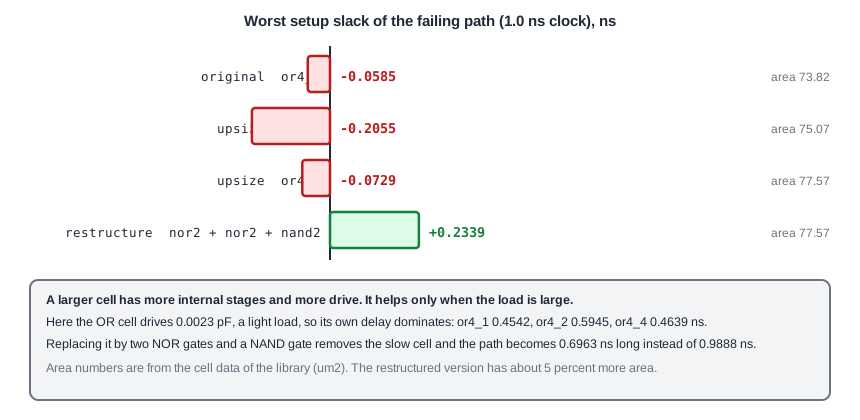
The design from Fixing Setup Violations has a failing path through a 4-input OR cell with a delay of 0.4542 ns. The slack is -0.0585 ns at a 1.0 ns clock. A first idea is to use a larger version of the cell. The results of replacing it by the larger cells of the library:
| Change | OR cell delay (ns) | Worst setup slack (ns) | Area (um2) |
|---|---|---|---|
| original, or4_1 | 0.4542 | -0.0585 | 73.82 |
| or4_2 | 0.5945 | -0.2055 | 75.07 |
| or4_4 | 0.4639 | -0.0729 | 77.57 |
| two NOR gates and a NAND gate | - | +0.2339 | 77.57 |
The larger OR cells are not faster. They have more internal stages and more drive strength, and drive strength only helps when the load is large. The load here is 0.0023 pF, a light one, so the delay of the cell itself decides, and a larger cell has a larger one. The restructured version, in which the OR of four signals is made from two NOR gates followed by a NAND gate, removes the slow cell, and the path becomes 0.6963 ns long instead of 0.9888 ns. The slack is +0.2339 ns, and the area is 3.75 um2 larger, about 5 percent.
A good tool tries both kinds of change and keeps the one that works. The lesson for the designer is to look at the delay of the cell and at its load in the report. A cell with a large delay and a small load needs a different structure, and a cell with a large load needs more drive.
Limits of Synthesis Timing
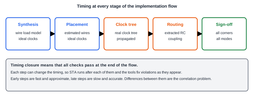
- No wires. The wire load model guesses the capacitance from the fanout. The real wires differ, and Pre-Layout and Post-Layout Timing Correlation shows by how much.
- No clock tree. The clocks are ideal, so skew is not in the numbers.
- No placement. A path that looks short can be spread over the chip.
- One corner, and often one mode.
Synthesis therefore leaves some margin: designers often give the synthesis tool a slightly faster clock than the real one, or add uncertainty, so that the result survives the later steps.
Common Mistakes
Mistake #1: Giving synthesis constraints that differ from sign-off
A path that is a false path in sign-off but not in synthesis wastes area, and a path that is optimized in synthesis with a missing exception can be over-constrained. Keep the files consistent, and review them together.
Mistake #2: Assuming a bigger cell is a faster cell
Size helps against a load. It does not help a path whose delay is mostly intrinsic. Look at the delay and the load of the cell before you change it.
Quick Check: A cell has a delay of 0.45 ns and drives a load of 0.002 pF. Is a larger version of the cell likely to help?
Probably not. The load is small, so the delay is mostly intrinsic, and a larger cell usually has a larger intrinsic delay.
Practice Exercise
Challenge: Work Out the Area Cost
This is a pencil and paper exercise. In the library, the area of or4_1 is 7.5072 um2 and the area of nor2_1 and of nand2_1 is 3.7536 um2 each. Calculate the area change when one or4_1 is replaced by two NOR gates and one NAND gate, and the relative change of a design with a total area of 73.82 um2.
Hint
The new cells together have three times 3.7536 um2.
Solution
The new cells have 3 x 3.7536 = 11.2608 um2. The change is 11.2608 - 7.5072 = 3.7536 um2, and the relative change is 3.7536 / 73.82 = 5.1 percent. For this price the setup slack of the path goes from -0.0585 ns to +0.2339 ns.
Summary
- Timing-driven synthesis uses the same constraints as STA: clocks, input and output delays, environment, exceptions and a wire model.
- The tool restructures logic, selects and sizes cells, adds buffers, duplicates gates and recovers area where the slack allows.
- A larger cell is not always faster. It helps against a load, and not against an intrinsic delay.
- On the example path, three small cells gave +0.2339 ns where two larger OR cells gave a worse result.
- The timing after synthesis has no real wires, clock tree or placement, so it is only an estimate.
- Keep the constraints of synthesis and of sign-off consistent.
