
Most of the timing of a chip is decided before any layout exists, in the RTL. An RTL structure that needs too many gates in series between two registers cannot be saved by the tools. A designer who knows what STA reports can write the RTL so that the paths are short. This article explains pipelining and retiming, shows them on an 8-bit adder with real numbers, and gives some coding habits that keep paths short.
9 min read | Intermediate
What You'll Learn
- Explain how the logic depth between registers sets the clock period
- Split a long path with a pipeline register and calculate the new clock limit
- Describe retiming and the balance of pipeline stages
- List the costs of pipelining and some RTL habits for shorter paths
Depth Sets the Clock
The clock period of a design has to cover the longest path between two registers: the clock-to-Q delay, the delays of all the gates in between, and the setup time. The more gates in series, the longer the period. For a given function, the structure that you describe in the RTL decides the number of levels, and synthesis can only reduce it by a limited amount.
An Example: an 8-Bit Adder
Here is an adder that adds two 8-bit numbers that come from registers, and stores the 9-bit result in a register:
module add1 (input clk, input [7:0] a, b, output reg [8:0] s);
  reg [7:0] ra, rb;
  always @(posedge clk) begin
    ra <= a;
    rb <= b;
    s <= ra + rb;
  end
endmodule
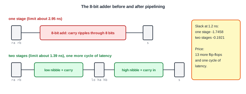
The carry has to ripple through the bits, and the path from the registers ra and rb to s is long. With a 1.2 ns clock, the worst setup slack is -1.7458 ns. The path needs about 1.2 + 1.7458 = 2.95 ns, and that is the shortest clock period of this design.
Pipelining
Pipelining puts a register in the middle of a long path, so that each half has a full clock period. In the adder, the low nibble and its carry are added in the first stage, and the high nibble in the second stage:
module add2 (input clk, input [7:0] a, b, output reg [8:0] s);
  reg [7:0] ra, rb;
  reg [4:0] lo; reg [3:0] ha, hb;
  always @(posedge clk) begin
    ra <= a;
    rb <= b;
    lo <= ra[3:0] + rb[3:0];          // stage 1: low nibble and its carry
    ha <= ra[7:4];
    hb <= rb[7:4];
    s <= {ha + hb + lo[4], lo[3:0]};   // stage 2: high nibble
  end
endmodule
| Design | Setup slack at 1.2 ns | Setup slack at 1.5 ns | Registers added |
|---|---|---|---|
| one stage | -1.7458 ns | -1.4458 ns | 0 |
| two stages | -0.1921 ns | +0.1079 ns | 13 |
The two-stage adder runs at 1.5 ns, and its shortest period is about 1.2 + 0.1921 = 1.39 ns. The clock can be more than twice as fast. The price is paid in other places:
- 13 more flip-flops (5 for the low nibble and its carry, and 8 for the high nibble inputs), which adds area and power.
- One more clock cycle of latency. The result appears one cycle later than before, and the rest of the design must be able to deal with it. This is a change in the behaviour, not only in the timing.
- The control logic and the data that goes with the result must be delayed in the same way, so that they stay aligned.
Quick Check
Q: A design runs at 2.0 ns. Its longest path of 1.8 ns is split by one register into 0.95 ns and 0.85 ns, each with the same overhead as before. About how fast can the clock be?
Show Answer
The limit becomes the longer half, 0.95 ns plus the overhead of a register stage (clock-to-Q and setup), so the period can be roughly 1.0 to 1.2 ns, depending on the overhead.
Balance the Stages
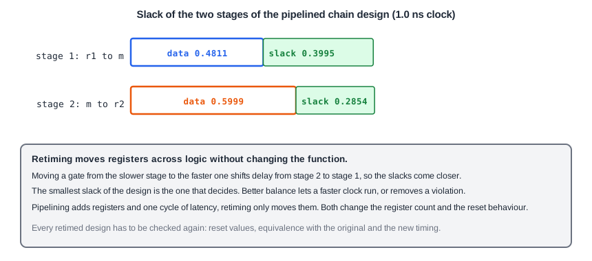
A pipeline is only as fast as its slowest stage. If one stage has 0.40 ns of slack and the other 0.29 ns, as in the pipelined chain design of the earlier articles (stage 1: 0.3995 ns, stage 2: 0.2854 ns at a 1.0 ns clock), the second stage is the limit. Moving a gate from the second stage to the first one makes the slacks equal and lets the clock run faster, or removes a violation of the slower stage.
Retiming does this automatically. It moves registers forward or backward across gates without changing the function seen from the outside. A tool can retime a design to balance the stages, but the registers it moves have a new meaning inside the design: the reset values and the visible signals of the original registers change. Designers use it when the structure is not a matter of function, and keep the registers whose names and reset values are used by software or by the verification environment.
Quick Check
Q: A pipeline has a setup slack of 0.3995 ns in stage 1 and 0.2854 ns in stage 2 at a 1.0 ns clock. What is its smallest clock period, and which stage sets it?
Show Answer
About 1.0 - 0.2854 = 0.7146 ns, set by stage 2, the one with the smaller slack. Moving logic from stage 2 to stage 1 would balance the stages and shorten the period.
RTL Habits for Short Paths
- Register the outputs of a block, and register the inputs of a block if the previous block is slow. A boundary of registers turns a long path into two short ones.
- Avoid long chains of
ifandelse ifwhen the conditions are exclusive. Acasestatement describes parallel logic. - Balance trees: sum or compare many values in a tree, not in a chain.
- Keep large multiplexers and wide comparisons close to registers, or split them over two cycles.
- Do not put a late-arriving signal at the start of the logic. Put it in the last level, where it only has to pass one gate.
- Look at the first synthesis report early. The worst paths show where the structure has to change.
Common Mistakes
Mistake #1: Pipelining without changing the rest of the design
The extra cycle of latency has to be accounted for in the control and in the data that belongs to the result. A pipeline register on the data only, without the same delay on the valid signal, gives wrong results.
Mistake #2: Adding registers to every path
Registers cost area, power and clock load. Pipeline the paths that limit the clock, and leave the others as they are.
Practice Exercise
Challenge: Find the Limit
Paste the add1 and the add2 designs into the lab with input delays of 0.1 ns on a and b and an output delay of 0.1 ns on s. Run both at 1.2 ns and note the worst setup slack. Predict the smallest clock period of each, and test your prediction for add2 at the period that you calculate.
Hint
For paths between registers, the slack changes by the same amount as the period. The smallest period is the period minus the worst slack.
Solution
The one-stage adder has a slack of -1.7458 ns at 1.2 ns, so its smallest period is about 1.2 + 1.7458 = 2.95 ns. The two-stage adder has -0.1921 ns, so its smallest period is about 1.2 + 0.1921 = 1.39 ns. At 1.5 ns, the two-stage design shows +0.1079 ns, which agrees. The cells chosen in the lab can differ, so your numbers may move a little, but the factor of about two is stable.
Open the ready-made example in the lab, run synthesis, and then run STA. Editing constraints.sdc and re-running only STA, and choosing another library or corner, are PRO features.
Summary
- The clock period has to cover the longest register-to-register path, and the RTL structure decides its depth.
- Pipelining splits a long path with registers. The 8-bit adder went from a limit of 2.95 ns to about 1.39 ns with 13 extra registers.
- The price is area, power and one more cycle of latency, which the rest of the design must handle.
- A pipeline is limited by its slowest stage, so the stages should be balanced.
- Retiming moves registers across logic automatically, and it changes the meaning of the registers inside.
- Write RTL with registered boundaries, parallel logic and balanced trees, and read the first timing report early.