
A large chip cannot be analyzed as one flat netlist in a single run. It has too many cells, and many teams work on different parts at the same time. Hierarchical STA divides the chip into blocks, analyzes each block on its own, and replaces it by a smaller model in the analysis of the top level. This article explains the three ideas behind it, budgets, extracted timing models and interface logic models, and shows a real extracted model of the demo circuit and how well it matches the full netlist.
9 min read | Intermediate
What You'll Learn
- Explain why large designs are analyzed hierarchically
- Describe timing budgets between blocks
- Read an extracted timing model and say what it contains
- Compare the result of a top-level run with a model against the full netlist
Why Divide the Chip
- Size: a flat run of a very large design needs a lot of memory and time.
- Teams: each block is designed by its own team, on its own schedule.
- Iteration: a change inside one block should not need a new analysis of the whole chip.
The price is that the blocks have to agree on the timing at their boundaries before they exist in their final form. This agreement is the budget.
Budgets
A budget splits the clock period of a path that crosses block boundaries. Take a path that starts in block A, goes through the top level, and ends in block B, with a clock period of 2.0 ns. If block A uses 0.9 ns, the top-level wires 0.2 ns and block B 0.7 ns, the sum is 1.8 ns and 0.2 ns is the margin. Each block team gets its share as constraints at its ports: an output delay for the part that is left after the block, and an input delay for the part that comes before it. These are the input and output delays of the chapter about SDC, and they are chosen so that the blocks can be designed independently.
A budget is a first guess. As blocks get implemented, the real delays are known and the budgets are updated, which is an iterative process between the top and the blocks.
Extracted Timing Models
When a block is finished, it is replaced for the top-level analysis by a timing model that has the same ports and the same timing at the ports, but no internal cells. An extracted timing model, ETM, is such a model. It is a library cell with timing arcs between the ports of the block, and it is written in the same Liberty format as the standard cells. OpenSTA can write one with write_timing_model:
read_liberty sky130_fd_sc_hd__tt_025C_1v80.lib
read_verilog netlist.v
link_design sta_demo
read_sdc demo.sdc
write_timing_model etm.lib
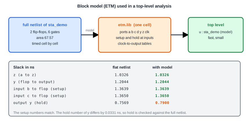
The model of the demo circuit contains one cell, sta_demo, marked as a macro, with these timing arcs:
- For each data input (
a,bandc), the setup and hold times relative to the clock. They include the logic inside the block between the input and its first flip-flop. Forb, the setup is 0.15013 ns for a rising and 0.23606 ns for a falling input, and the hold times are -0.12699 and -0.17832 ns. - For the output
y, which comes from a flip-flop through a gate, a clock-to-output delay table as a function of the load. For a load of 0.0005 pF the rising delay is 0.40147 ns, and for 0.10896 pF it is 1.43352 ns. - For the output
z, which is a combinational path from the inputsaandd, the delay tables of those arcs. - The clock pin with the clock tree delay of the block, 0.0 here because the clocks are ideal.
How Well the Model Matches
To test the model, a top level that instantiates the block, module top with the cell sta_demo as u, was analyzed with the library of the model and the same constraints as the flat design. The slacks of the main paths:
| Path | Flat netlist (ns) | With the model (ns) |
|---|---|---|
| input a to output z (setup) | 1.0326 | 1.0326 |
| flip-flop to output y (setup) | 1.2044 | 1.2044 |
| input b to flip-flop (setup) | 1.3639 | 1.3639 |
| input c to flip-flop (setup) | 1.3650 | 1.3650 |
| output y (hold) | 0.7569 | 0.7900 |
The setup slacks are the same to four digits. The hold slack of the output y differs by 0.0331 ns, which is why hold should be checked on the full netlist. The report of the path from a to z shows the block as a single cell:
   0.4000    0.4000 v input external delay
   0.0000    0.4000 v a (in)
   0.1674    0.5674 v u/z (sta_demo)
   0.0000    0.5674 v z (out)
Interface Logic Models
An extracted timing model hides everything inside the block. A different kind of model, an interface logic model, ILM, keeps the part of the netlist that is connected to the ports, the logic between the ports and the first or last registers, and discards the rest. The ILM is a real netlist with the internal register-to-register paths removed. It keeps the exact timing at the boundary, including the effects of the real cells and the crosstalk to the top level, and it is smaller than the full block. It is more accurate than an ETM and bigger.
Using Models in a Flow
- The chip planner makes budgets for every block, as input and output delays and as clock latencies.
- Each block is implemented and analyzed on its own with those constraints.
- When a block is stable, a model is written for it, an ETM or an ILM, for all the corners and modes.
- The top level is analyzed with the models of the blocks, which is fast and small, and with its own cells and wires.
- The violations at the boundaries are fixed by changing the budgets or the blocks, and the loop is repeated.
- At sign-off, a full flat run of the whole design is often done as a last check, because the models are approximations.
Common Mistakes
Mistake #1: Using a model made at a different corner
A timing model holds numbers for one corner. A top-level analysis at another corner needs the model of that corner, or the result is wrong. Make one model for each scenario.
Mistake #2: Treating a budget as a final result
A budget is a guess about delays that do not exist yet. If a block is implemented and the real delays exceed the budget, the budgets have to be changed, and the top level analyzed again.
Quick Check: What does an extracted timing model contain, and what does it leave out?
It contains the timing arcs and the setup and hold values at the ports of the block, in Liberty form. It leaves out the internal cells and wires, so that the top level analysis is smaller and faster.
Practice Exercise
Challenge: Split a Budget
This is a pencil and paper exercise. A path crosses block A, the top level and block B, in a design with a 2.0 ns clock. Block A uses a clock-to-output delay of 0.85 ns and block B has an input-to-register path of 0.65 ns plus a setup time of 0.10 ns. The wires at the top level take 0.30 ns. Find the slack, and find which output delay you would give block A so that the top-level wires may use up to 0.40 ns.
Hint
The slack is the period minus all the delays on the path. The output delay of block A is everything after block A.
Solution
The sum of the delays is 0.85 + 0.30 + 0.65 + 0.10 = 1.90 ns, so the slack is 2.0 - 1.90 = 0.10 ns. If the top-level wires may use 0.40 ns, the part after block A is 0.40 + 0.65 + 0.10 = 1.15 ns, so block A gets an output delay of 1.15 ns. Its own path then has 2.0 - 1.15 = 0.85 ns, which is the delay it already has, so the slack of that path is 0.
Summary
- Hierarchical STA analyzes the blocks of a large chip separately and uses models of them in the top-level run.
- A budget splits the clock period between blocks and the top level, as input and output delays.
- An extracted timing model is a Liberty cell with arcs between the ports. OpenSTA writes it with
write_timing_model. - For the demo circuit, the top-level slacks with the model match the flat netlist to four digits for setup. The hold slack of
ydiffers by 0.0331 ns. - An interface logic model keeps the logic at the boundary and drops the rest, so it is more accurate than an ETM.
- Models are made per corner and mode, and a flat sign-off run is the last check.
