
A single port RAM is a memory with one address port, so it can read or write one location per clock cycle, but not both at different addresses at once. In Verilog, the storage is declared as an array of registers, a clocked always block writes it when write enable is high, and another clocked block reads from it when write enable is low.
12 min read | Beginner Level
What You'll Learn
- How a single port RAM is organized and controlled with address, data and enable signals
- Write a parameterized single port RAM with synchronous write and synchronous read
- How memory arrays are inferred as RAM blocks during synthesis, and what prevents it
- Test the RAM by writing and reading back every location
What is a single port RAM ?
A single port RAM is a digital memory that reads from or writes to one memory location at a time. Each location, selected by an address, stores a fixed number of bits called a word, usually a power of 2 such as 8, 16 or 32 bits. A read returns the word stored at an address, and a write stores a new word at an address, replacing the old one.
The size of a RAM is described by its depth, the number of words, and its width, the number of bits per word. A RAM with 16 words of 32 bits is called a 16 x 32 RAM and holds 512 bits. The number of address bits needed is $clog2(depth), so 16 words need 4 address bits.
Why is it called single port ?
A port is a set of address and data connections through which the memory is accessed. A single port RAM has only one, so in any clock cycle it performs either one read or one write, never both. If a write is in progress, a read must wait, and the reverse.
A dual port RAM has two independent address ports, so it can, for example, write one location while reading another in the same cycle. That flexibility costs area: a single port memory cell is smaller, so single port RAMs are used wherever reads and writes never need to happen together.
Signals
A single port RAM is controlled through three groups of signals:
- Address lines select the location. With N address lines, up to 2N locations can be addressed.
- Data lines carry the word being written into or read out of the selected location.
- Control signals start and qualify each operation. The design below uses three:
cs(chip select) enables the memory,we(write enable) chooses write over read, andoe(output enable) lets the memory drive the data bus.
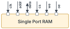
| cs | we | oe | Operation at the clock edge | data bus |
|---|---|---|---|---|
| 0 | x | x | None (memory idle) | High impedance |
| 1 | 1 | x | Write data to mem[addr] | Driven by the testbench or bus master |
| 1 | 0 | 1 | Read mem[addr] | Driven by the RAM |
| 1 | 0 | 0 | Read into the output register | High impedance |
Verilog Design
The design uses a single bidirectional data bus, declared as inout. The RAM drives it only during a read with output enable set, and releases it to high impedance (z) at all other times, so the other side can drive it during writes.
module single_port_sync_ram
  # (parameter ADDR_WIDTH = 4,
     parameter DATA_WIDTH = 32,
     parameter DEPTH = 16               // Number of words; normally 2**ADDR_WIDTH
    )

  ( 	input 					clk,
   		input [ADDR_WIDTH-1:0]	addr,
   		inout [DATA_WIDTH-1:0]	data,
   		input 					cs,		// Chip Select
   		input 					we,		// Write Enable
   		input 					oe		// Output Enable
  );

  reg [DATA_WIDTH-1:0] 	tmp_data;       // Read data register
  reg [DATA_WIDTH-1:0] 	mem [0:DEPTH-1];   // Storage: DEPTH words of DATA_WIDTH bits

  // Synchronous write: store the bus value at the clock edge
  always @ (posedge clk) begin
    if (cs & we)
      mem[addr] <= data;
  end

  // Synchronous read: capture the addressed word at the clock edge
  always @ (posedge clk) begin
    if (cs & !we)
    	tmp_data <= mem[addr];
  end

  // Drive the bus only while reading with output enabled; release it otherwise
  assign data = cs & oe & !we ? tmp_data : 'hz;
endmodule

Both the write and the read happen on the rising clock edge. A read therefore has a latency of one clock cycle: the address is sampled at one edge, and the word appears on tmp_data, and on the bus if oe is set, after that edge.
Synthesis result: Synthesis tools recognize an array written in a clocked block and read into a register as a RAM. On an FPGA, the tool maps it to a block RAM, or to distributed LUT RAM for small sizes. For an ASIC, the RAM is usually generated by a memory compiler and instantiated, while this RTL serves as its simulation model. The tri-state driver on data is a separate concern: it is only implemented as real hardware at chip pins, as explained below.
Quick Check
Q: The address is set to 5 and a read is requested just before a rising clock edge. When is the word from location 5 available on tmp_data?
Show Answer
Right after that clock edge. The read block captures mem[5] into tmp_data at the edge, so logic clocked by the same clock can use the data at the following edge. This one-cycle read latency is typical of synchronous RAMs, including FPGA block RAMs.
Where are Single Port RAMs Used?
Processor caches are built from large single port SRAM arrays: in each cycle, the cache either looks up a line for a read or fills a line after a miss, so one port is enough. Using single port cells instead of dual port cells keeps the cache, often the largest block on the chip, as small as possible.
Separate Read and Write Data Ports
Inside a chip, the common style is to give the RAM a separate input data bus and output data bus instead of one inout bus. It is still a single port RAM, because there is only one address, but no tri-state logic is needed:
module spram #(parameter ADDR_WIDTH = 4, DATA_WIDTH = 32) (
  input                       clk,
  input                       we,
  input      [ADDR_WIDTH-1:0] addr,
  input      [DATA_WIDTH-1:0] din,
  output reg [DATA_WIDTH-1:0] dout
);

  reg [DATA_WIDTH-1:0] mem [0:(1<<ADDR_WIDTH)-1];   // Depth follows ADDR_WIDTH

  always @(posedge clk) begin
    if (we)
      mem[addr] <= din;        // Write
    else
      dout <= mem[addr];       // Read, registered: block RAM friendly
  end

endmodule
This is the pattern FPGA synthesis tools document for inferring block RAM, and it maps directly onto the ports of an ASIC memory macro.
Video Line Buffers
Image processing blocks, such as scalers and filters, store one or more lines of pixels in on-chip RAM so that they can use neighboring pixels from the line above. Each line buffer is a RAM with one word per pixel, written as pixels arrive and read when the next line is processed.
Verilog Testbench
The testbench writes a random value to every location, then reads every location back. During writes it sets oe to 0 and drives the shared bus itself; during reads it sets oe to 1 and releases the bus, so the RAM can drive it.
module tb;
  parameter ADDR_WIDTH = 4;
  parameter DATA_WIDTH = 16;
  parameter DEPTH = 16;

  reg clk;
  reg cs;
  reg we;
  reg oe;
  reg [ADDR_WIDTH-1:0] addr;
  wire [DATA_WIDTH-1:0] data;
  reg [DATA_WIDTH-1:0] tb_data;
  integer i;

  single_port_sync_ram #(.ADDR_WIDTH(ADDR_WIDTH), .DATA_WIDTH(DATA_WIDTH), .DEPTH(DEPTH)) u0
  ( 	.clk(clk),
                        	.addr(addr),
                        	.data(data),
                        	.cs(cs),
   							.we(we),
   							.oe(oe)
                         );

  always #10 clk = ~clk;

  // The testbench drives the bus only while the RAM's output is disabled
  assign data = !oe ? tb_data : 'hz;

  initial begin
    {clk, cs, we, addr, tb_data, oe} <= 0;

    repeat (2) @ (posedge clk);

    // Write a random word to every location
    for (i = 0; i < 2**ADDR_WIDTH; i= i+1) begin
      @(posedge clk);
      addr <= i; we <= 1; cs <=1; oe <= 0; tb_data <= $random;
    end

    // Read every location back
    for (i = 0; i < 2**ADDR_WIDTH; i= i+1) begin
      @(posedge clk);
      addr <= i; we <= 0; cs <= 1; oe <= 1;
    end

    #20 $finish;
  end
endmodule
All the signals for one access change together on a clock edge, and the RAM acts on them at the next edge. In the waveform, each word written during the first loop appears on data during the second loop, one cycle after its address is applied.
Quick Check
Q: In the testbench, what would happen if assign data = !oe ? tb_data : 'hz; were replaced by assign data = tb_data;?
Show Answer
During reads, both the testbench and the RAM would drive data at the same time. Wherever the two values differ, the bus resolves to x, so the read data is corrupted. Exactly one side may drive a shared bus at any time; the other must drive z.
Packet Buffers in Network Devices
Network switches and interface controllers store incoming packets in on-chip RAM until they can be forwarded. Writes and reads are scheduled so they never collide, which allows single port memories, sometimes split into several banks so that one bank can be written while another is read.
Common Beginner Mistakes
Mistake #1: Reading the memory asynchronously
Wrong: assign dout = mem[addr];
Right: Register the read data: always @(posedge clk) dout <= mem[addr];
Why? FPGA block RAMs and most memory macros only support synchronous reads. An asynchronous read cannot be mapped to them, so the tool builds the memory from distributed LUT RAM or, for larger sizes, from thousands of flip-flops and a huge read mux. The design works in simulation, but uses far more area and is much slower.
Mistake #2: Resetting the whole memory array
Wrong: if (!rstn) for (i = 0; i < DEPTH; i = i + 1) mem[i] <= 0;
Right: Do not reset the array; reset only the control logic, and initialize contents through writes or an initialization file
Why? RAM blocks have no way to clear every word at once, so a reset loop forces the tool to build the memory from flip-flops. If the contents must be known after reset, clear them with a sequence of writes, or use a valid bit per entry.
Mistake #3: Driving the shared bus from both sides
Wrong: A testbench or bus master that drives data continuously, or a RAM that drives it during writes
Right: Each side drives data only in its own phase and drives 'hz otherwise
Why? Two drivers on one net produce x wherever their values differ, which corrupts both reads and writes. Inside a chip, avoid inout buses entirely and use separate din and dout, because internal tri-state buses are not supported on FPGAs and are avoided in ASIC design.
Mistake #4: DEPTH that does not match ADDR_WIDTH
Wrong: ADDR_WIDTH = 4 with DEPTH = 10, while the address can still reach 15
Right: Use DEPTH = 2**ADDR_WIDTH, or keep every address below DEPTH
Why? A write to an address beyond the array is ignored in simulation, and a read returns x, so data is silently lost. In hardware, the result depends on how the tool sizes the memory. Deriving the depth from the address width, as spram does, avoids the mismatch.
Practice Exercise
Challenge: Self-Checking RAM Testbench
Write a testbench for spram (with ADDR_WIDTH = 4 and DATA_WIDTH = 16) that writes a random value to every address, keeps a copy of each value in a testbench array, then reads every address back and compares the result with the copy. Print each mismatch and a pass or fail summary.
Hint
Remember the one-cycle read latency: set the address at one clock edge, then check dout after the next edge. Comparing on the falling edge after the read edge avoids races with the RAM's register update.
Solution
module tb_check;
  reg         clk = 0;
  reg         we;
  reg  [3:0]  addr;
  reg  [15:0] din;
  wire [15:0] dout;
  reg  [15:0] expected [0:15];       // Reference copy of the memory
  integer     i, errors;

  spram #(.ADDR_WIDTH(4), .DATA_WIDTH(16)) u0
    (.clk(clk), .we(we), .addr(addr), .din(din), .dout(dout));

  always #10 clk = ~clk;

  initial begin
    errors = 0;
    we = 0; addr = 0; din = 0;

    // Write phase
    for (i = 0; i < 16; i = i + 1) begin
      @(negedge clk);
      we = 1; addr = i; din = $random;
      expected[i] = din;                // Remember what was written
    end

    // Read phase: address applied before an edge, data checked after it
    for (i = 0; i < 16; i = i + 1) begin
      @(negedge clk);
      we = 0; addr = i;
      @(negedge clk);                   // The rising edge in between performs the read
      if (dout !== expected[i]) begin
        $display("ERROR: addr=%0d read=%h expected=%h", i, dout, expected[i]);
        errors = errors + 1;
      end
    end

    if (errors == 0) $display("PASS: all 16 locations read back correctly");
    else             $display("FAIL: %0d mismatches", errors);
    $finish;
  end
endmodule
Inputs change on the falling edge, so they are stable at every rising edge where the RAM acts. Using !== also catches x values, which would appear if a location had never been written or if the address went out of range.
Summary
In this tutorial, you learned:
- A single port RAM has one address port, so it performs either one read or one write per cycle
- Its size is described by depth and width, and it needs
$clog2(depth)address bits - In Verilog, the storage is an array such as
reg [W-1:0] mem [0:DEPTH-1] - Synchronous write and registered read let synthesis map the array to block RAM or a memory macro
- A synchronous read has a latency of one clock cycle
- A shared
inoutbus needs exactly one driver at a time; inside a chip, separatedinanddoutare preferred - Asynchronous reads and array resets prevent RAM inference and cost large amounts of logic
