
12 min read | Beginner Level
What You'll Learn
- What synthesis is and what a gate-level netlist looks like
- How constraints guide synthesis, and what a constraint file contains
- Which Verilog constructs are not synthesizable, and which RTL patterns become which hardware
- Why x and z comparisons and multiple drivers cause problems in synthesis
What is synthesis ?
Synthesis is the process of turning a high-level description of a circuit, written in Verilog, into a lower-level representation that can be built in an FPGA or an ASIC. The result is usually a netlist: a list of gates, flip-flops and other cells from a target library, and the wires that connect them.
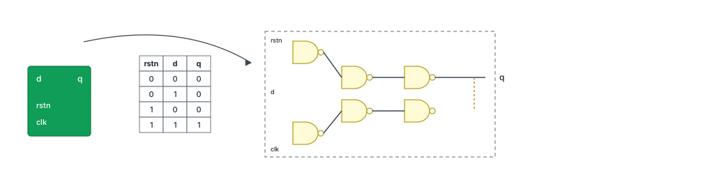
Synthesis maps the abstract behavior of the design, such as "add these two numbers on every clock edge", onto real hardware components, and optimizes the result for area, timing and power. For an ASIC, the components are standard cells such as NAND gates and flip-flops; for an FPGA, they are look-up tables (LUTs), flip-flops, carry chains, block RAMs and DSP blocks.
As an example, here is a 2-bit counter and a netlist that synthesis could produce for it:
module cnt2 (input clk, rstn, output reg [1:0] q);
  always @(posedge clk or negedge rstn)
    if (!rstn) q <= 0;
    else       q <= q + 1;
endmodule
// Netlist after synthesis (cell names are illustrative)
module cnt2 (clk, rstn, q);
  input        clk, rstn;
  output [1:0] q;
  wire         n0, n1;

  INV  U1 (.A(q[0]), .Y(n0));                          // Next value of bit 0
  XOR2 U2 (.A(q[1]), .B(q[0]), .Y(n1));                // Next value of bit 1
  DFFR q_reg_0_ (.D(n0), .CK(clk), .RN(rstn), .Q(q[0]));
  DFFR q_reg_1_ (.D(n1), .CK(clk), .RN(rstn), .Q(q[1]));
endmodule
The always block with posedge clk became two flip-flops with an asynchronous reset, and q + 1 became one inverter and one XOR gate, which is all a 2-bit increment needs. The netlist is still Verilog, but it only instantiates library cells, as described in Verilog Gate Level Modeling.
How is synthesis done ?
Synthesis works on a synthesizable subset of Verilog, usually written at the register transfer level (RTL). The tool goes through roughly these steps:
- Elaboration: reads the RTL, resolves parameters and generate blocks, and builds the design hierarchy.
- Translation: turns each construct into generic logic: registers, multiplexers, adders, comparators and Boolean equations.
- Optimization: simplifies the logic, removes unused and duplicate gates, and restructures it to reduce the number of gates and improve performance.
- Technology mapping: implements the optimized logic with the cells of the target library, choosing faster or smaller cells so that the timing constraints are met.
The output is a gate-level netlist, usually with reports on area, timing and power. Different synthesis tools can interpret some Verilog constructs slightly differently, so the same code can give different results with different tools; staying within the commonly supported subset avoids most of these differences.
The table below shows what common RTL patterns become in hardware, with links to the articles that explain them:
| RTL pattern | Synthesized hardware |
|---|---|
always @(posedge clk) q <= d; | D flip-flop |
assign y = sel ? b : a; or a complete case | Multiplexer, see 4 to 1 mux |
if ... else if ... else | Priority logic, see priority encoder |
a + b, a - b, a * b | Adder, subtractor, multiplier |
a == b, a < b | Comparators |
Combinational always block that does not assign an output in every path | Latch, usually unintended, see D latch |
for loop with constant bounds | Replicated logic, one copy per iteration |
What is a synthesis constraint file ?
RTL describes what the hardware does, but not how fast it must be. That information comes from a constraint file, usually written in the SDC (design constraints) format, which is supported by most synthesis and timing tools. It specifies the clocks, the timing of the inputs and outputs, and limits on area, power and fanout, and synthesis uses it to decide how hard to optimize each path.
# Set the version of the SDC file
set sdc_version 2.1

# Define the clock
create_clock -period 10 [get_ports clk]  ; # 100 MHz clock

# Set input delay constraints
set_input_delay -max 2 [get_ports data_in[*]] -clock [get_clocks clk]
set_input_delay -min 1 [get_ports data_in[*]] -clock [get_clocks clk]

# Set output delay constraints
set_output_delay -max 3 [get_ports data_out[*]] -clock [get_clocks clk]
set_output_delay -min 1 [get_ports data_out[*]] -clock [get_clocks clk]

# Set load capacitance on output ports
set_load 0.01 [get_ports data_out[*]]

# Define false paths (if any)
set_false_path -from [get_ports reset] -to [get_ports data_out[*]]

# Set maximum fanout for specific ports
set_max_fanout 10 [get_ports data_in[*]]
create_clockdefines a clock with a period of 10 ns, so every path between flip-flops must be faster than that.set_input_delaytells the tool that inputs arrive 1 to 2 ns after the clock edge, leaving the rest of the period for the logic inside the design.set_output_delayreserves time after the outputs for the logic in the receiving device.set_false_pathexcludes a path that does not have to meet timing, such as from a slow reset input.
Synthesis result: The same RTL can produce very different netlists depending on the constraints. With a relaxed clock, an adder may be built as a small, slow ripple-carry chain; with a tight clock, the tool picks a larger, faster structure and stronger cells.
Quick Check
With the constraints above, how much of the 10 ns clock period is left for logic between an input pin and the first flip-flop, in the worst case?
Show Answer
8 ns, minus the flip-flop's setup time. The maximum input delay of 2 ns is already used outside the design, before the signal reaches the input pin.
Verilog Constructs to Avoid
Not all Verilog constructs can be synthesized. Many exist only to write testbenches and models. Synthesizable code should stay within the constructs that the tools support:
| Construct | Description |
|---|---|
| Initial Blocks | Used for testbenches; not synthesizable for ASICs and ignored during synthesis. Many FPGA tools accept simple initial assignments as power-up values of registers and memories. |
| Delay Constructs | Delays such as #10 are simulation-only and ignored by synthesis. |
| Real Data Types | real, realtime and time are not synthesizable. |
| Fork/Join Constructs | fork and join are not supported in synthesis. |
| Random Functions | Random number functions like $random are not synthesizable. |
| X and Z States | Comparisons against x and z cannot be built in hardware. z is only supported to describe tri-state buffers. |
| Primitives | Gate primitives are supported; switch primitives and user-defined primitives are not. |
| Force and Release | force and release on data types are not supported. |
| Event and Wait Controls | wait, named events and @ in the middle of a block are not synthesizable; only the event control at the top of an always block is. |
| Loops with Variable Bounds | while, forever and for loops whose number of iterations is not known at compile time cannot be unrolled into hardware. |
| System Tasks | $display, $monitor, $finish and file I/O are ignored. |
Support for some constructs differs between tools, so check the documentation of the tool you use. A useful rule is to write synthesizable RTL as if describing the hardware directly: registers, the combinational logic between them, and the connections.
Separate RTL and Testbench Code
Projects keep synthesizable RTL and testbench code in separate directories, and only the RTL directory is given to synthesis. Lint tools check the RTL for non-synthesizable constructs before every synthesis run, so that a stray #5 or $display is caught early instead of silently being ignored.
Comparison of X and Z
In simulation, x means unknown and z means not driven. Real hardware only has voltages that a gate reads as 0 or 1, so a circuit cannot test whether a wire is "unknown". Synthesis tools therefore treat comparisons against x and z as always false, or as "don't care", and the intended logic is not built.
module compare_xz (
    input wire b,
    output reg a
);
    always @(*) begin
        if ((b === 1'bz) || (b === 1'bx)) begin
            a = 1; // Set a to 1 if b is high impedance or unknown
        end else begin
            a = 0; // Set a to 0 otherwise
        end
    end
endmodule
In simulation, the case equality operator === compares x and z bits exactly, so a becomes 1 whenever b is x or z. In the synthesized hardware, b is always 0 or 1, both comparisons are false, and a becomes a constant 0: the module is reduced to a wire tied to ground. The simulation and the hardware disagree.
With the normal equality operator ==, the comparison does not even work in simulation: b == 1'bz gives x, which an if treats as false. Either way, logic that depends on detecting x or z cannot be built. Keep synthesizable code to the binary values 0 and 1, avoid comparisons with x and z, and make sure every signal is driven to a defined value, for example with a reset.
Quick Check
What hardware does synthesis build for compare_xz?
Show Answer
Only a constant: output a is tied to 0, and input b is not used at all. Synthesis tools usually report that the input is unconnected and that the comparisons were treated as false.
Multiple Driver
A net or variable that is assigned from more than one place has multiple drivers. In hardware, that means two outputs connected to the same wire, which can fight each other. Synthesis cannot decide which source should win and reports an error.
module multiple_drivers_example (
    input wire clk,
    input wire reset,
    input wire enable,
    output reg out
);

    // First driver
    always @(posedge clk or posedge reset) begin
        if (reset) begin
            out <= 0; // Reset condition
        end
    end

    // Second driver
    always @(posedge clk) begin
        if (enable) begin
            out <= 1; // Another assignment to out
        end
    end

endmodule
Both always blocks assign out, so synthesis reports a "multiple drivers" error: each block would need its own flip-flop driving the same output. Simulation, on the other hand, accepts the code and simply uses whichever assignment happens last, which can hide the problem until synthesis. The fix is to describe each register in exactly one always block, with all of its conditions:
always @(posedge clk or posedge reset) begin
  if (reset)
    out <= 0;          // Reset has priority
  else if (enable)
    out <= 1;
end
Synthesis result: The fixed code becomes one flip-flop with an asynchronous reset. Its D input is enable | out: once enable has been 1, the output stays 1 until the next reset.
Synthesis-Simulation Mismatch Reviews
A mismatch between RTL simulation and the synthesized netlist is one of the most expensive bugs in chip design, because all RTL tests pass while the real chip behaves differently. Teams guard against it with lint checks for the usual causes, such as x comparisons, multiple drivers, incomplete sensitivity lists and inferred latches, and with formal equivalence checking, which proves mathematically that the netlist implements the RTL.
Common Beginner Mistakes
Mistake #1: Creating a latch by accident
Wrong:
always @(*) begin
  if (en) y = a;        // No else: y must keep its value when en = 0
end
Right: Assign y in every path, for example with else y = 0;, or a default assignment at the top of the block
Why? If a combinational block does not assign an output in every case, the output has to remember its old value, and synthesis builds a latch. Latches complicate timing analysis and are almost never what was intended in an @(*) block.
Mistake #2: Relying on initial blocks for reset values in ASIC designs
Wrong: initial count = 0; as the only way to give a register its starting value
Right: Use a reset: if (!rstn) count <= 0;
Why? ASIC synthesis ignores initial blocks, so the register powers up with a random value, while simulation shows 0. Some FPGA tools accept initial values, but a reset works on every target.
Mistake #3: Using delays to fix timing
Wrong: assign #2 y = a & b; to make the hardware wait
Right: Describe the logic without delays and give timing requirements in the constraint file
Why? Synthesis ignores delays. The actual timing is decided by the cells, the layout and the constraints, and checked with static timing analysis.
Mistake #4: Assigning a register from two always blocks
Wrong: One block for the reset and another block for the normal update, as in multiple_drivers_example
Right: Put the reset and every other condition for that register in one always block
Why? Synthesis rejects the multiple drivers, while simulation runs anyway, so the problem appears late. One register, one block is the rule that avoids it.
Practice Exercise
Challenge: Make It Synthesizable
The module below simulates, but cannot be synthesized as intended. Find the problems and rewrite it as synthesizable RTL with an active-low reset.
module pulse_count (input clk, rstn, pulse, output reg [7:0] count);
  initial count = 0;

  always @(posedge clk)
    if (pulse === 1'bx) count = count;
    else if (pulse)     #1 count = count + 1;

  always @(negedge rstn)
    count = 0;
endmodule
Hint
Look for an initial block, an x comparison, a delay, blocking assignments in a clocked block, and two blocks that assign the same register.
Solution
module pulse_count (input clk, rstn, pulse, output reg [7:0] count);
  always @(posedge clk or negedge rstn)
    if (!rstn)      count <= 0;
    else if (pulse) count <= count + 1;
endmodule
The initial block is replaced by the reset, the x comparison is removed because hardware never sees x, the #1 delay is removed, the assignments are nonblocking, and the reset is merged into the same block so that count has only one driver. Synthesis builds an 8-bit register with asynchronous reset and an incrementer, with pulse as the enable.
Summary
In this tutorial, you learned:
- Synthesis turns RTL into a gate-level netlist of library cells, optimized for area, timing and power
- The flow goes through elaboration, translation to generic logic, optimization and technology mapping
- Constraint files in SDC format give the clocks and I/O timing that guide optimization
- Initial blocks, delays, real types, fork/join, $random, force/release, wait and variable-bound loops are not synthesizable
- Comparisons with x and z cannot be built in hardware and cause mismatches between simulation and synthesis
- Each register must be assigned from exactly one always block, and combinational blocks must assign every output in every path to avoid latches
