
The previous article introduced the built-in gate primitives such as and, or, xor and not. This article puts them to work on four classic combinational circuits: a multiplexer, a full adder, a decoder and a priority encoder. To write Verilog code with gates, you first need to know how the gates connect, so each example starts from the Boolean equation and the schematic, and then translates them line by line into primitives.
12 min read | Beginner Level
What You'll Learn
- Turn a Boolean equation into a gate-level Verilog module, one primitive per gate
- Build a 2x1 mux, a full adder, a 2x4 decoder and a 4x2 priority encoder from primitives
- Read the simulation logs to check each circuit against its truth table
- What synthesis does with gate-level code, and the common mistakes in these circuits
Example #1: 2x1 Multiplexer
A 2x1 multiplexer passes one of two inputs to its output, chosen by a select line. In this version, sel = 1 picks a and sel = 0 picks b:
out = (a & sel) | (b & ~sel)
That equation needs one NOT gate for ~sel, two AND gates (one per data path) and one OR gate to merge the two paths.
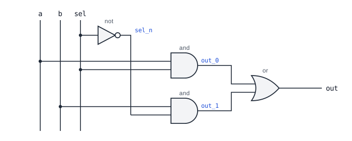
module mux_2x1 ( input a, b, sel,
                 output out);
  wire sel_n;     // Inverted select
  wire out_0;     // a path, active when sel = 1
  wire out_1;     // b path, active when sel = 0

  not (sel_n, sel);

  and (out_0, a, sel);
  and (out_1, b, sel_n);

  or (out, out_0, out_1);
endmodule
The output port out is a wire by default, which is what a primitive output needs. At any time only one AND gate can be enabled, so the OR gate simply forwards whichever path is active.
This mux uses the opposite select convention from the mux2_gate example in the previous article, where sel = 0 picked a. Neither is wrong, but always check which input the select picks before you connect a mux someone else wrote.
The testbench drives random values onto the three inputs once every time unit. $random returns a 32-bit number, and assigning it to a 1-bit reg keeps only the lowest bit, so each input gets a random 0 or 1.
module tb;
  reg a, b, sel;
  wire out;
  integer i;

  mux_2x1 u0 ( .a(a), .b(b), .sel(sel), .out(out));

  initial begin
    {a, b, sel} <= 0;

    $monitor ("T=%0t a=%0b b=%0b sel=%0b out=%0b", $time, a, b, sel, out);

    for (i = 0; i < 10; i = i+1) begin
      #1  a <= $random;
          b <= $random;
          sel <= $random;
    end
  end
endmodule
ncsim> run
T=0 a=0 b=0 sel=0 out=0
T=1 a=0 b=1 sel=1 out=0
T=2 a=1 b=1 sel=1 out=1
T=3 a=1 b=0 sel=1 out=1
T=6 a=0 b=1 sel=0 out=1
T=7 a=1 b=1 sel=0 out=1
T=8 a=1 b=0 sel=0 out=0
T=9 a=0 b=1 sel=0 out=1
T=10 a=1 b=1 sel=1 out=1
ncsim: *W,RNQUIE: Simulation is complete.
At T=1, sel = 1 picks a = 0, so out = 0 even though b = 1. At T=6, sel = 0 picks b = 1. T=4 and T=5 are missing because the random values happened to repeat, and $monitor only prints when something changes.
Synthesis result: The four primitives describe a 2 to 1 multiplexer. A synthesis tool usually recognizes the pattern and maps it to a single MUX2 cell from the library, or into part of a LUT on an FPGA, rather than keeping four separate gates. The gate-level code fixes the function, not the final cells.
Quick Check
With a = 1, b = 0 and sel = 0, what are out_0, out_1 and out?
Show Answer
out_0 = a & sel = 0, out_1 = b & sel_n = 0 & 1 = 0, so out = 0. With sel = 0 the mux forwards b, which is 0. This is the T=8 line of the log.
Full Adder
A full adder adds three 1-bit inputs, a, b and a carry in cin, and produces a 1-bit sum and a carry out cout:
sum  = a ^ b ^ cin
cout = (a & b) | (cin & (a ^ b))
The term a ^ b appears in both equations, so it is computed once into the internal wire s1 and shared. net1 is the carry that a and b generate on their own, and net2 is the carry that passes through from cin when exactly one of a and b is 1.
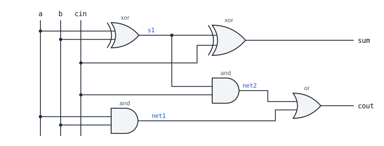
module fa ( input a, b, cin,
            output sum, cout);

  wire s1, net1, net2;

  xor (s1, a, b);         // s1 = a ^ b, shared by sum and cout
  and (net1, a, b);       // Carry generated by a and b

  xor (sum, s1, cin);     // sum = a ^ b ^ cin
  and (net2, s1, cin);    // Carry propagated from cin

  or (cout, net1, net2);

endmodule
module tb;
  reg a, b, cin;
  wire sum, cout;
  integer i;

  fa u0 ( .a(a), .b(b), .cin(cin),
          .sum(sum), .cout(cout));

  initial begin
    {a, b, cin} <= 0;

    $monitor ("T=%0t a=%0b b=%0b cin=%0b cout=%0b sum=%0b",
              $time, a, b, cin, cout, sum);

    for (i = 0; i < 10; i = i+1) begin
      #1  a <= $random;
          b <= $random;
          cin <= $random;
    end
  end
endmodule
ncsim> run
T=0 a=0 b=0 cin=0 cout=0 sum=0
T=1 a=0 b=1 cin=1 cout=1 sum=0
T=2 a=1 b=1 cin=1 cout=1 sum=1
T=3 a=1 b=0 cin=1 cout=1 sum=0
T=6 a=0 b=1 cin=0 cout=0 sum=1
T=7 a=1 b=1 cin=0 cout=1 sum=0
T=8 a=1 b=0 cin=0 cout=0 sum=1
T=9 a=0 b=1 cin=0 cout=0 sum=1
T=10 a=1 b=1 cin=1 cout=1 sum=1
ncsim: *W,RNQUIE: Simulation is complete.
Read {cout, sum} as a 2-bit number and it is the count of 1s among the inputs. At T=2 all three inputs are 1, so {cout, sum} = 11, which is 3. At T=1 two inputs are 1, giving 10, which is 2.
Synthesis result: Synthesis produces two XOR-type cells and an AND-OR structure for the carry, often merged into a single AND-OR-INVERT or majority cell. Many standard cell libraries also contain a dedicated full adder cell, and the tool may replace all five gates with that one cell. On an FPGA, the adder maps onto the LUT and the dedicated carry chain.
Quick Check
For a = 1, b = 1 and cin = 0, what are s1, net1, net2, sum and cout?
Show Answer
s1 = 1 ^ 1 = 0, net1 = 1 & 1 = 1, net2 = 0 & 0 = 0, sum = 0 ^ 0 = 0 and cout = 1 | 0 = 1. One plus one gives binary 10, which matches the T=7 line of the log.
Adders in Every Datapath
The full adder is the building block of the adders in a processor's ALU, address calculation units and counters. Chaining N full adders, with each cout feeding the next cin, gives an N-bit ripple carry adder. Faster adders used in high-speed datapaths reorganize the same generate (a & b) and propagate (a ^ b) signals that appear here as net1 and s1.
2x4 Decoder
A 2x4 decoder turns a 2-bit input code into four outputs, where exactly one output is 1 for each code. An enable input en forces every output to 0 when it is low. Each output is a 3-input AND of en with the true or inverted form of x and y:
| en | x | y | a | b | c | d |
|---|---|---|---|---|---|---|
| 0 | X | X | 0 | 0 | 0 | 0 |
| 1 | 0 | 0 | 0 | 0 | 0 | 1 |
| 1 | 0 | 1 | 0 | 0 | 1 | 0 |
| 1 | 1 | 0 | 0 | 1 | 0 | 0 |
| 1 | 1 | 1 | 1 | 0 | 0 | 0 |
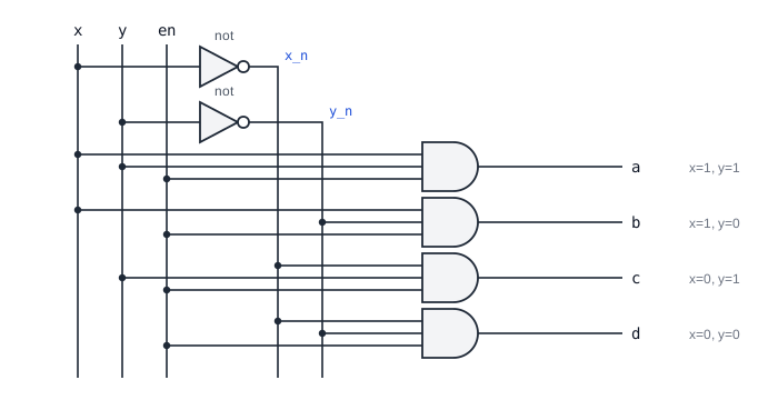
module dec_2x4 ( input x, y, en,
                 output a, b, c, d);

  wire x_n, y_n;

  not (x_n, x);
  not (y_n, y);

  and (a,  x,   y,   en);    // Code 11
  and (b,  x,   y_n, en);    // Code 10
  and (c,  x_n, y,   en);    // Code 01
  and (d,  x_n, y_n, en);    // Code 00

endmodule
Note that the output names run in the opposite order to the codes: d is active for code 00 and a for code 11. The testbench sets en to 1 and then applies random codes.
module tb;
  reg x, y, en;
  wire a, b, c, d;
  integer i;

  dec_2x4 u0 ( .x(x), .y(y), .en(en),
               .a(a), .b(b), .c(c), .d(d));

  initial begin
    {x, y, en} <= 0;
    $monitor ("T=%0t x=%0b y=%0b en=%0b a=%0b b=%0b c=%0b d=%0b",
              $time, x, y, en, a, b, c, d);

    en <= 1;
    for (i = 0; i < 10; i = i+1) begin
      #1  x <= $random;
          y <= $random;
    end
  end
endmodule
ncsim> run
T=0 x=0 y=0 en=1 a=0 b=0 c=0 d=1
T=1 x=0 y=1 en=1 a=0 b=0 c=1 d=0
T=2 x=1 y=1 en=1 a=1 b=0 c=0 d=0
T=4 x=1 y=0 en=1 a=0 b=1 c=0 d=0
T=5 x=1 y=1 en=1 a=1 b=0 c=0 d=0
T=6 x=0 y=1 en=1 a=0 b=0 c=1 d=0
T=7 x=1 y=0 en=1 a=0 b=1 c=0 d=0
T=10 x=1 y=1 en=1 a=1 b=0 c=0 d=0
ncsim: *W,RNQUIE: Simulation is complete.
The log already shows en=1 at T=0 because both nonblocking assignments to en happen in the same time step, and the later one wins before $monitor prints. Every line has exactly one output at 1, which is the defining property of a decoder.
Synthesis result: Synthesis keeps the structure of two inverters and four 3-input AND functions, but the exact cells depend on the library. A common mapping uses NOR or NAND cells with the inverters absorbed, since x_n & y_n is the same as ~(x | y).
Quick Check
If the testbench never set en to 1, what would the outputs show?
Show Answer
All four outputs would stay 0 for every value of x and y, because en is an input to every AND gate. When a decoder output never goes high, check the enable first.
Address Decoding
On a system bus, the upper address bits pass through a decoder to produce one select signal per peripheral, such as a timer, a UART and a GPIO block. Only the selected peripheral responds to a read or write. The enable input is driven by a "bus transaction valid" signal, so no peripheral is selected while the bus is idle. Memory arrays use the same idea on a larger scale to select one word line out of thousands.
4x2 Priority Encoder
An encoder does the reverse of a decoder: it converts which input is active into a binary code. A priority encoder also decides what happens when several inputs are active at once, by reporting the one with the highest priority. Here d has the highest priority and a the lowest:
| d | c | b | a | x | y |
|---|---|---|---|---|---|
| 1 | X | X | X | 1 | 1 |
| 0 | 1 | X | X | 1 | 0 |
| 0 | 0 | 1 | X | 0 | 1 |
| 0 | 0 | 0 | X | 0 | 0 |
Reading the table column by column gives the equations:
x = d | c
y = d | (b & ~c)
x is 1 whenever one of the two upper inputs is active. y is 1 for d, or for b as long as c does not override it. Input a does not appear in either equation, because its code 00 is what the outputs show when nothing above it is active.
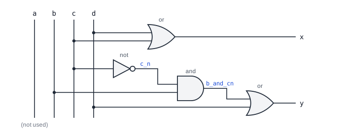
module enc_4x2 ( input a, b, c, d,
                 output x, y);

  wire c_n;        // ~c
  wire b_and_cn;   // b & ~c

  // x = d | c
  or  (x, d, c);

  // y = d | (b & ~c)
  not (c_n, c);
  and (b_and_cn, b, c_n);
  or  (y, d, b_and_cn);

endmodule
The testbench counts through every combination of the four inputs by assigning the loop variable to the concatenation {a, b, c, d}, so a is the most significant bit.
module tb;
  reg a, b, c, d;
  wire x, y;
  integer i;

  enc_4x2 u0 ( .a(a), .b(b), .c(c), .d(d), .x(x), .y(y));

  initial begin
    {a, b, c, d} <= 0;

    $monitor("T=%0t a=%0b b=%0b c=%0b d=%0b x=%0b y=%0b",
             $time, a, b, c, d, x, y);

    for (i = 0; i <= 16; i = i+1) begin
      #1 {a, b, c, d} <= i;
    end
  end

endmodule
ncsim> run
T=0 a=0 b=0 c=0 d=0 x=0 y=0
T=2 a=0 b=0 c=0 d=1 x=1 y=1
T=3 a=0 b=0 c=1 d=0 x=1 y=0
T=4 a=0 b=0 c=1 d=1 x=1 y=1
T=5 a=0 b=1 c=0 d=0 x=0 y=1
T=6 a=0 b=1 c=0 d=1 x=1 y=1
T=7 a=0 b=1 c=1 d=0 x=1 y=0
T=8 a=0 b=1 c=1 d=1 x=1 y=1
T=9 a=1 b=0 c=0 d=0 x=0 y=0
T=10 a=1 b=0 c=0 d=1 x=1 y=1
T=11 a=1 b=0 c=1 d=0 x=1 y=0
T=12 a=1 b=0 c=1 d=1 x=1 y=1
T=13 a=1 b=1 c=0 d=0 x=0 y=1
T=14 a=1 b=1 c=0 d=1 x=1 y=1
T=15 a=1 b=1 c=1 d=0 x=1 y=0
T=16 a=1 b=1 c=1 d=1 x=1 y=1
T=17 a=0 b=0 c=0 d=0 x=0 y=0
ncsim: *W,RNQUIE: Simulation is complete.
There are a few details worth reading in this log:
- There is no T=1 line, because the loop applies
i = 0at T=1, which is the same value as before. - At T=8,
b,canddare all 1, and the output is11becausedwins. - At T=7,
bandcare both 1, andcwins with10. - At T=17,
i = 16is5'b10000, and only its lower 4 bits fit into{a, b, c, d}, so the inputs wrap back to 0000.
Synthesis result: x maps to a single 2-input OR cell. y = d | (b & ~c) is a classic AND-OR shape, which synthesis usually implements as one complex AND-OR-INVERT cell plus an inverter, rather than three separate gates. Input a drives nothing, so the tool removes it from the logic and may report it as an unused input.
Because a = 1 alone and "no input active" both give xy = 00, a real priority encoder usually adds a valid output that tells the two cases apart. With gates it takes one more output port, output valid, and one more primitive:
  // valid = 1 when at least one input is active
  or (valid, a, b, c, d);
For the RTL way of writing priority logic with if-else-if and casez, and for wider encoders, see Verilog Priority Encoder.
Quick Check
Without the valid output, can you tell the input a = 1, b = 0, c = 0, d = 0 apart from all inputs at 0?
Show Answer
No. Both give x = 0 and y = 0, as the T=9 and T=17 lines of the log show. Only a separate valid output, which is 1 when any input is active, separates "a is active" from "nothing is active".
Interrupt Controllers
When several peripherals raise interrupt requests at the same moment, an interrupt controller uses a priority encoder to choose which one the processor handles first. The encoder's code becomes the interrupt number, and the valid output tells the processor that an interrupt is pending at all. Arbiters that grant a shared bus to one of several requesters use the same priority logic.
Common Beginner Mistakes
Mistake #1: Assuming which input the mux select picks
Wrong: Connecting mux_2x1 with the default path on a, expecting sel = 0 to pick a
Right: Read the gates: and (out_0, a, sel) means a passes when sel = 1
Why? There is no standard rule for which mux input belongs to sel = 0. With gate-level code, the AND gate that receives sel rather than sel_n tells you which input is selected by 1. Getting it backwards produces a design that compiles and simulates, but passes the wrong data.
Mistake #2: A typo in an internal wire name
Wrong:
  wire sel_n;
  not (sel_n, sel);
  and (out_1, b, seln);      // Typo: seln is not declared
Right: Use the declared name sel_n, and add `default_nettype none at the top of the file so that undeclared names are reported as errors
Why? Verilog creates an implicit 1-bit wire for an undeclared name used in a port connection. seln has no driver, so it stays at z, the AND gate outputs x or 0, and the mux silently stops passing b. In gate-level code with many internal wires, this is one of the most common bugs.
Mistake #3: Forgetting the decoder enable
Wrong: Leaving en at 0 or unconnected in the testbench, then debugging why a, b, c and d never change
Right: Drive en to 1, as the testbench does with en <= 1;
Why? The enable is an input to every AND gate, so it masks all four outputs. An unconnected input port is z, which makes the AND outputs x or 0, never a clean 1.
Mistake #4: Using an encoder without a valid output
Wrong: Treating xy = 00 from enc_4x2 as "input a is active"
Right: Add or (valid, a, b, c, d); and only use x and y when valid is 1
Why? The lowest priority input and "no input" share the same code. An interrupt controller without a valid output would service interrupt 0 even when no interrupt is pending.
Mistake #5: A testbench loop that wraps around
Wrong: for (i = 0; i <= 16; i = i+1) #1 {a, b, c, d} <= i;, then wondering why the inputs return to 0000 at the end
Right: Use i < 16 to cover the 16 combinations of a 4-bit value exactly once
Why? Assigning a wider value to a narrower target keeps only the lower bits. 16 is 10000 in binary, so {a, b, c, d} receives 0000. It does no harm here, but in other testbenches the extra wrapped value can trigger unexpected behavior or hide that a case was never tested.
Practice Exercise
Challenge: 2-Bit Equality Comparator
Write a module eq_2bit with inputs a1, a0, b1 and b0, and an output eq that is 1 when the 2-bit numbers {a1, a0} and {b1, b0} are equal. Use only gate primitives, and test all 16 input combinations.
Hint
Two bits are equal when their XNOR is 1. The numbers are equal when both bit pairs are equal, so combine the two XNOR outputs with an AND gate.
Solution
module eq_2bit ( input a1, a0, b1, b0,
                 output eq);

  wire e1, e0;

  xnor (e1, a1, b1);     // 1 when the upper bits match
  xnor (e0, a0, b0);     // 1 when the lower bits match
  and  (eq, e1, e0);     // Equal only if both bits match

endmodule

module tb;
  reg a1, a0, b1, b0;
  wire eq;
  integer i;

  eq_2bit u0 (.a1(a1), .a0(a0), .b1(b1), .b0(b0), .eq(eq));

  initial begin
    $monitor("T=%0t a=%0b%0b b=%0b%0b eq=%0b", $time, a1, a0, b1, b0, eq);
    for (i = 0; i < 16; i = i+1) begin
      {a1, a0, b1, b0} = i;
      #1;
    end
  end
endmodule
eq is 1 for exactly four combinations: 00/00, 01/01, 10/10 and 11/11, which are i = 0, 5, 10 and 15. The loop uses i < 16, so there is no wrapped value at the end. A wider comparator adds one XNOR per bit and a wider AND gate, and synthesis builds the same structure from the RTL expression a == b.
Summary
In this tutorial, you learned:
- A gate-level module starts from the Boolean equation: one primitive per gate and one
wireper internal connection - The 2x1 mux uses NOT, two ANDs and an OR; which input
sel = 1picks is set by which AND gate receivessel - The full adder shares
a ^ bbetweensumandcout, and the carry is generate OR propagate - The 2x4 decoder ANDs the enable with each combination of true and inverted inputs, so exactly one output is 1
- The 4x2 priority encoder reduces to
x = d | candy = d | (b & ~c), and needs a valid output to tell inputafrom no input - Synthesis keeps the function of gate-level code but is free to remap it to MUX, full adder or complex AND-OR cells
