
Most digital chips contain analog blocks: PLLs that make the clocks, references and regulators that set voltages, sensors, and data converters. Their behaviour cannot be fully predicted before silicon, and many need calibration on every part. This article describes what is measured on PLLs and analog blocks, how converters are characterized, and how trimming with fuses adjusts each part to its target.
6 min read | Intermediate
What You'll Learn
- List the key measurements of a PLL on silicon
- Describe the main specifications of a data converter
- Explain trimming and why many analog blocks need it
- Use on-chip analog test access
PLLs
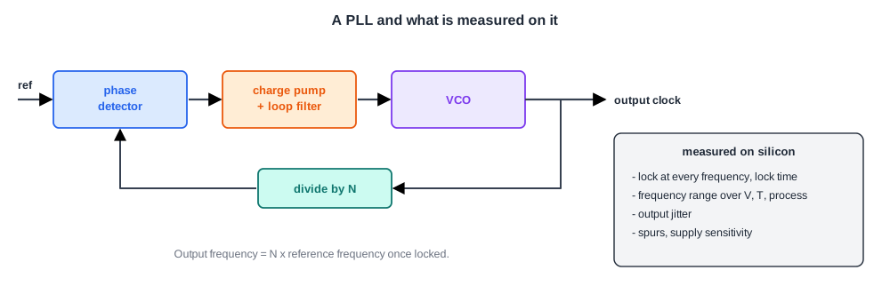
A phase-locked loop multiplies a reference clock up to the chip's operating frequencies. Validation measures:
- Lock: whether it locks at every required frequency, and how long it takes.
- Frequency range: the lowest and highest frequencies it can reach, across voltage, temperature and process.
- Jitter: how much the output edges wander, which eats directly into every timing path's margin.
- Spurs and supply sensitivity: unwanted tones in the output and how much supply noise reaches the clock.
Many chips bring a divided clock out to a pin or measure it with an on-chip counter, so these can be measured without probing the die.
Quick Check
Q: Why does PLL jitter matter for digital timing, not just for analog performance?
Show Answer
Every timing path depends on the clock edges arriving on time. Jitter moves edges, so a cycle can be shorter than nominal, reducing setup margin on every path. Timing sign-off includes a jitter allowance, and silicon must show the real jitter fits inside it.
Data Converters

Analog-to-digital and digital-to-analog converters are characterized with static and dynamic measurements:
- Differential nonlinearity (DNL): how much each code step differs from the ideal step width. A DNL of -1 means a missing code.
- Integral nonlinearity (INL): how far the transfer curve bends away from a straight line.
- Signal-to-noise ratio and effective bits: measured with a pure sine wave input. The effective number of bits is (SNR - 1.76) / 6.02, with SNR in decibels.
Converters are sensitive to supply noise and substrate noise from the digital logic around them, so they are measured both alone and with the digital part of the chip busy, as the Physical Design article Analog and Mixed-Signal Blocks in a Digital Chip explains.
Trimming
Many analog values vary too much from part to part to be fixed in design: a bandgap reference voltage, an oscillator frequency, a temperature sensor's offset, a regulator's output. These blocks are made adjustable, and each part is trimmed.
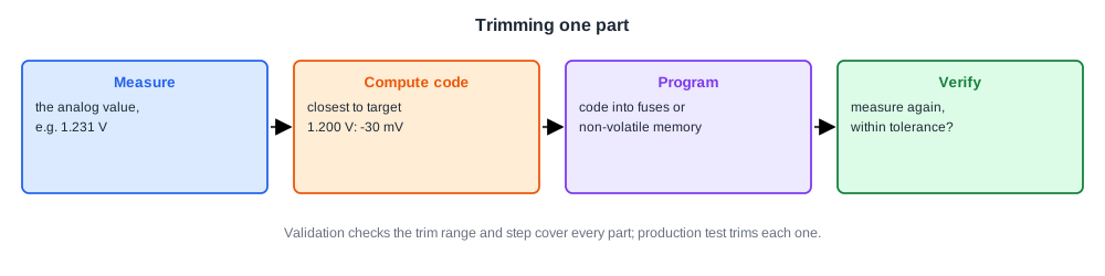
- Measure the value on the part.
- Compute the trim code that brings it closest to the target.
- Program the code into fuses or non-volatile memory.
- Measure again to verify.
Validation decides whether the trim range and step size are enough: does every part, across the process, land within specification after trimming? Production test then trims every part.
Quick Check
Q: A reference voltage should be 1.200 V. Untrimmed parts range from 1.170 V to 1.240 V, and the trim adjusts in 5 mV steps over ±30 mV. Can every part be trimmed to within ±2.5 mV?
Show Answer
No. Parts need corrections from +30 mV to -40 mV, but the trim only reaches -30 mV, so the 1.240 V parts end at 1.210 V.
The range must grow or the design must reduce the spread. Within range, 5 mV steps can reach within ±2.5 mV.
Analog Test Access
Analog nodes inside the chip are hard to measure. Many chips include an analog test bus: switches that route a chosen internal node, such as a reference voltage or a regulator output, to a pin where an instrument can measure it. Some I/O libraries provide analog buses through the pad ring for the same purpose, and digital readouts of on-chip sensors let software see analog values without any instrument at all.
In Practice
Analog validation is usually done by the analog designers themselves, with specialized instruments and a lot of statistics across parts and temperatures. Its results feed trim programs, datasheet limits and sometimes changes to the digital side: for example, quieting nearby logic during a converter's sampling window.
Common Mistakes
Mistake #1: Measuring a converter with the digital logic idle only
Digital noise degrades converters. Measure with the chip busy too.
Mistake #2: Too little trim range
Check trim range against the full process spread, including corner parts.
Mistake #3: No access to internal analog nodes
Plan an analog test bus or readouts before tapeout.
Practice Exercise
Challenge: Effective Bits
A 12-bit ADC measures an SNR of 68 dB with a sine wave input. What is its effective number of bits? What SNR would a perfect 12-bit converter have?
Hint
ENOB = (SNR - 1.76) / 6.02.
Solution
ENOB = (68 - 1.76) / 6.02 = 11.0 bits. A perfect 12-bit converter has SNR = 6.02 x 12 + 1.76 = 74.0 dB. About one bit is lost to noise and distortion, a common result that is checked against the specification.
Summary
- PLLs are checked for lock, frequency range, jitter, spurs and supply sensitivity; jitter consumes timing margin.
- Converters are characterized by DNL, INL, SNR and effective bits, with the digital logic quiet and busy.
- Many analog values are trimmed per part through fuses; validation checks the trim range covers the process spread.
- Analog test buses and sensor readouts give access to internal analog nodes.
