
Physical failure analysis looks directly at the silicon to find where and why a circuit fails: measuring voltages on internal nodes, seeing light or heat from faulty transistors, and cutting or adding wires to test a theory. It is used when the electrical and logical evidence points to a region but cannot settle the exact cause. This article describes the main techniques, from mechanical probes to focused ion beams, what each can see, and when it is used.
7 min read | Advanced
What You'll Learn
- Describe probe pads and mechanical probing
- Explain electron-beam and laser voltage probing
- Use emission and thermal imaging to find faults
- Explain how a focused ion beam edits a chip
Mechanical Probing
Designers can bring key internal signals up to small squares of top metal, about 5 to 10 µm on a side, with an opening in the passivation above them. Under a microscope, a fine-tipped probe can contact these pads.
The probe loads the node. A typical high-end probe adds about 50 fF of capacitance, so the design may need a buffer in front of the pad to avoid slowing the circuit being measured. Probe pads must be planned before tapeout.
Beam and Laser Probing
When mechanical contact is not possible, the die can be probed without touching it:
- Electron-beam probing scans a focused electron beam over the circuit and measures on-chip voltages.
- Laser voltage probing shines a laser on a transistor and measures the reflected light, which is modulated by the electric fields, so switching waveforms can be reconstructed. It can be invasive: the light can disturb sensitive dynamic nodes.
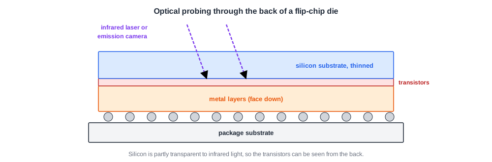
Silicon is partly transparent to infrared light, so laser probing works through the back of the die. That matters for flip-chip packages, where the metal layers face the package and block access from the front.
Quick Check
Q: Why are optical techniques used from the backside of flip-chip parts?
Show Answer
In a flip-chip package the front of the die, with its metal layers, faces the package and is covered by bumps. The transistors are only reachable through the silicon substrate, which infrared light can pass through, usually after the substrate has been thinned.
Seeing Light and Heat
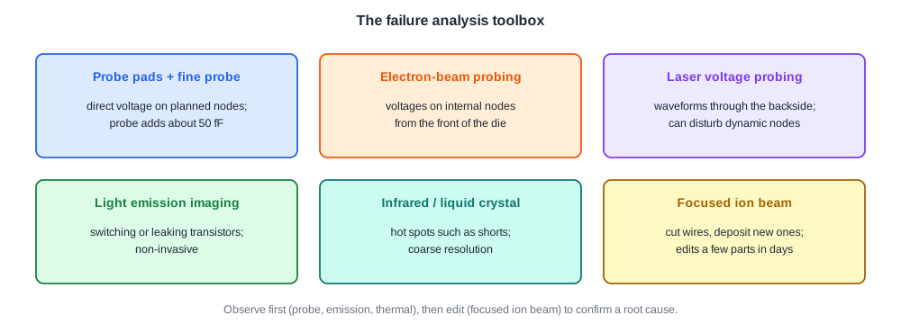
- Emission imaging captures the faint light that transistors give off when they switch, or when they leak abnormally. Time-resolved versions record when each transistor switches, without disturbing the circuit.
- Thermal imaging with infrared cameras finds hot spots, for example a resistive short between supply rails.
- Liquid crystal painted on the die changes appearance with temperature, giving a coarse view of hot regions.
These are often the first step for a defect: a short or a leaking gate shows up as a bright or hot spot, which tells the analyst where to look.
Quick Check
Q: A part draws 200 mA more standby current than normal. Which technique quickly finds where?
Show Answer
Thermal imaging or emission imaging. The extra current flows through a small region, such as a short or a damaged gate, which gets hotter and may emit light. The hot spot or emission site locates the defect for closer inspection.
Editing With a Focused Ion Beam
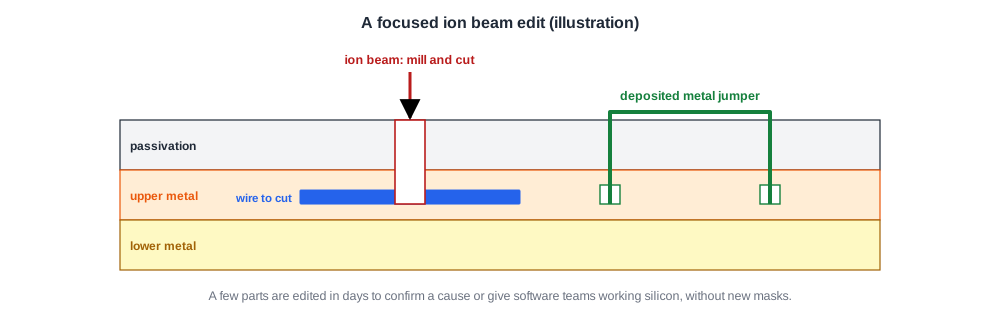
A focused ion beam can cut wires and deposit new conductors on a finished chip. If the fault and the fix are known, a few parts can be edited and tested in days, instead of waiting weeks for new masks.
Edits confirm a root cause: if cutting a coupling wire or adding a buffer makes the failure go away, the theory is right. They also give working parts to software teams before the fixed stepping arrives. Plastic packages can be ground open to reach the die.
A Worked Example
A published case involved a dynamic multiplexer that failed only at certain voltages, in an odd shmoo shape. Its select line was supposed to stay high, but laser voltage probing showed it being pulled low.
The cause was coupling: one neighbour wire and many wires running over the top of the select line all fell at about the same time. Noise analysis had only checked side neighbours. The fix was to make the select line static, which resists coupling.
In Practice
Failure analysis labs are specialized and expensive, and some techniques destroy the part. Analysts get the best results when debug has already narrowed the fault to a block and a node. Deeper physical analysis, removing layers one at a time and imaging with an electron microscope, is used for defects and reliability failures, especially those from field returns.
Common Mistakes
Mistake #1: Sending a part to failure analysis with no localization
Narrow the fault to a block and node first; the techniques are slow over large areas.
Mistake #2: Forgetting probe loading
A probe on an unbuffered node can change the behaviour being measured.
Mistake #3: Ignoring invasive effects of laser probing
Light can disturb dynamic nodes. Cross-check with a non-invasive method.
Practice Exercise
Challenge: Probe Loading
A node is driven through an effective 2 kΩ and normally has 30 fF of load. A probe adds 50 fF.
Estimate the RC delay before and after probing. What does this suggest about probing this node directly?
Hint
RC delay is roughly R x C.
Solution
Before: 2 kΩ x 30 fF = 60 ps. After: 2 kΩ x 80 fF = 160 ps, more than double. Probing it directly would slow the circuit enough to change its timing, so a buffer in front of the probe pad, or a non-contact method, is needed.
Summary
- Probe pads let fine probes measure internal nodes, but the probe load must be planned for.
- Electron-beam and laser voltage probing measure waveforms without contact, laser often through the backside.
- Emission, infrared and liquid crystal imaging locate switching, leaking or hot spots.
- Focused ion beam edits cut and add wires on a few parts to confirm causes and fixes.
