
Electrostatic discharge and latch-up are two ways a chip can be destroyed through its pins. A static discharge from a person or a machine can put thousands of volts on a pin for a few nanoseconds. Latch-up turns on a parasitic path between the supplies that can carry enough current to melt wires.
Both are designed against in the I/O ring and layout, and both are checked on silicon by deliberately zapping and over-driving pins. This article covers the models used, the protection structures and the tests.
6 min read | Intermediate
What You'll Learn
- Describe the human body and charged device ESD models
- Explain how pad protection circuits divert ESD current
- Explain the parasitic structure behind latch-up
- Describe how ESD and latch-up are tested on silicon
ESD Models
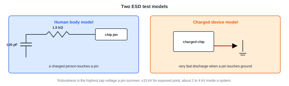
Test standards model two common events:
- Human body model: a charged person touches a pin. A 100 pF capacitor charged to a high voltage discharges into the pin through 1.5 kΩ.
- Charged device model: the chip itself becomes charged, for example while sliding through handling equipment, then discharges very fast when a pin touches ground. It is harder to protect against.
Robustness is quoted as the highest voltage a pin survives. Parts exposed to users, such as ports on cables, may need ±15 kV. Parts inside an enclosed system, exposed only during assembly, typically need around 2 to 4 kV.
Protection Circuits
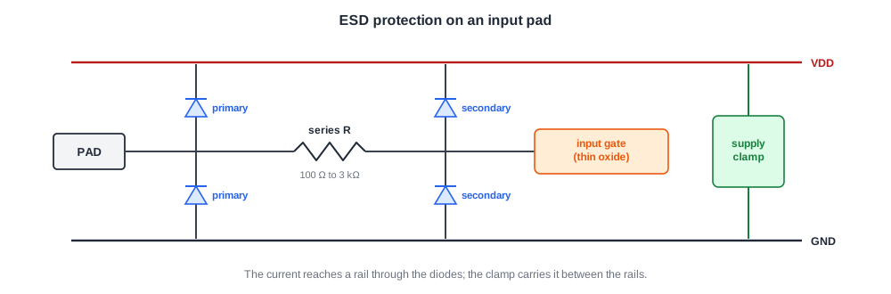
Every pad has a path to carry ESD current safely to a supply rail before it reaches thin gate oxides:
- Primary diodes from the pad to each supply clamp large voltages.
- A series resistor, typically 100 Ω to 3 kΩ, limits current to the inner circuit, with secondary diodes clamping further.
- Supply clamps between the rails carry the current once it reaches a supply.
Protection adds capacitance and resistance, which high-speed and analog pads must balance against bandwidth.
Quick Check
Q: A human body model zap at 2 kV discharges through 1.5 kΩ. What is the peak current, roughly?
Show Answer
About 2,000 / 1,500 = 1.3 A, for a time set by 1.5 kΩ x 100 pF = 150 ns. The protection diodes and clamps must carry over an ampere without the pad voltage rising high enough to damage the gate oxides.
Latch-Up
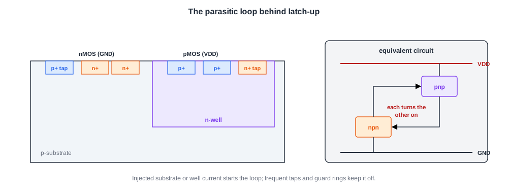
The wells and diffusions of CMOS form two parasitic bipolar transistors connected in a loop between the supply and ground. Normally both are off. If enough current flows in the substrate or well, for example when a pin rings below ground or above the supply, one turns on, which turns on the other, and the pair latches into a low-resistance path.
The current persists until power is removed, and can melt wires. Prevention relies on frequent substrate and well taps, and on guard rings around I/O transistors that can inject current. Silicon-on-insulator processes and supplies below about 1.4 to 2 V are largely immune, but I/O supplies are often higher.
Quick Check
Q: Why are I/O pads the most likely place to trigger latch-up?
Show Answer
External signals can ring below ground or above the supply, forward-biasing junctions and injecting current into the substrate or well. Inside the chip, voltages stay between the rails. Guard rings around I/O transistors collect that current before it triggers the parasitic loop.
Testing on Silicon
- ESD: pins are zapped with the human body and charged device models at increasing voltages, in all pin combinations required by the standard. After each step the part is tested for function and leakage to find the failure threshold.
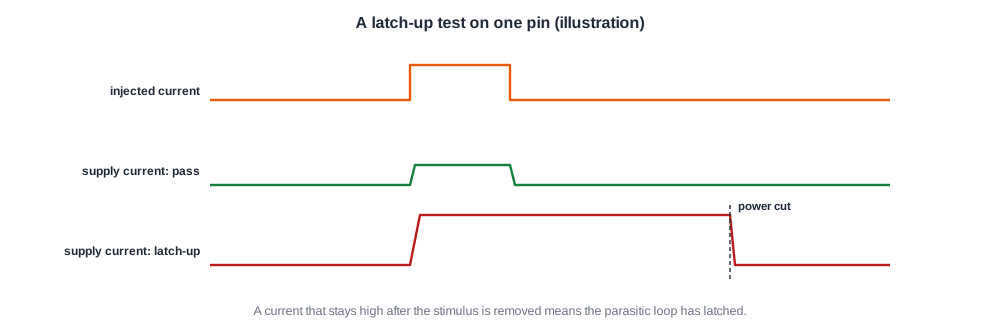
- Latch-up: each pin is driven with injected current or overvoltage, at high temperature, while supply current is monitored. A sustained jump in current that stays after the stimulus is removed means latch-up.
In Practice
ESD and latch-up results are part of reliability qualification. Failing pins go to failure analysis, where thermal and emission imaging often show the damaged device.
Fixes usually need layout changes in the pad ring, so problems found late can force a stepping. That is why ESD design rules and checks are strict before tapeout.
Common Mistakes
Mistake #1: Testing only the human body model
Charged device events are faster and fail differently. Test both.
Mistake #2: Weak protection on high-speed pads
Reducing protection for bandwidth must still meet the ESD target.
Mistake #3: Latch-up tests at room temperature only
Latch-up is easier to trigger when hot. Test at high temperature.
Practice Exercise
Challenge: ESD Energy
A 100 pF capacitor is charged to 4 kV for a human body model test. How much energy does it store? If the protection lets 5 % of it reach an inner node, how much energy is that?
Hint
E = C V2 / 2.
Solution
E = 100 x 10-12 x (4,000)2 / 2 = 0.8 mJ. 5 % is 40 µJ, delivered in nanoseconds, far more than a thin gate oxide can absorb. Protection must divert almost all of it.
Summary
- Human body and charged device models represent the two common ESD events.
- Pad diodes, series resistors and supply clamps divert ESD current away from gate oxides.
- Latch-up is a parasitic SCR triggered by injected current; taps and guard rings prevent it.
- Silicon tests zap pins and inject current at high temperature to find failure thresholds.
