
A universal gate is a gate type that can build any Boolean function on its own, with no help from other gate types. NAND and NOR are the two universal gates. In CMOS they are also the cheapest gates to build, because a single transistor stage naturally produces an inverted output. That is why NAND, NOR, and inverters sit at the heart of every standard-cell library, and why a circuit described with ANDs and ORs usually ends up in silicon as NANDs.
14 min read | Beginner Level
What You'll Learn
- Why NAND and NOR can build every other gate, and why AND and OR cannot
- How to build NOT, AND, OR, and XOR from only NAND or only NOR gates
- A reliable method for converting any expression to a NAND-only or NOR-only circuit
- Why CMOS cell libraries lean on NAND gates, and what that means for synthesis results
What Makes a Gate Universal?
NAND is AND followed by NOT: its output is 0 only when all inputs are 1. NOR is OR followed by NOT: its output is 1 only when all inputs are 0.
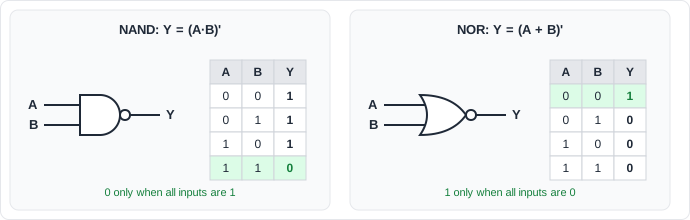
The argument for universality has two steps. First, the set {AND, OR, NOT} can express any truth table: write one AND term for every row where the output is 1, then OR the terms together. Second, if one gate type can build AND, OR, and NOT, it can build anything those three can build.
Can the gate build ...      NOT    AND    OR     Universal?
  AND alone                 no     yes    no     no
  OR alone                  no     no     yes    no
  AND + OR together         no     yes    yes    no
  NAND alone                yes    yes    yes    YES
  NOR alone                 yes    yes    yes    YES
The missing ingredient for AND and OR is inversion. In any circuit built only from AND and OR gates, changing an input from 0 to 1 can never change the output from 1 to 0. NOT needs exactly that, so no combination of AND and OR can produce it. NAND and NOR carry an inversion inside them, which is exactly what makes them universal.
Quick Check
Q: Is XOR a universal gate on its own?
Show Answer
No. XOR can build NOT if a constant 1 is available (A XOR 1 = A'), but no combination of XOR gates can build AND. XOR circuits can only produce functions that are XORs of their inputs, and AB is not one of them.
Building Basic Gates from NAND
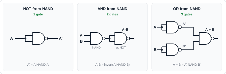
NOT :  A'     = A NAND A                          1 gate
AND :  A . B  = (A NAND B) NAND (A NAND B)        2 gates  (NAND, then a NAND used as NOT)
OR  :  A + B  = (A NAND A) NAND (B NAND B)        3 gates  (invert both inputs, then NAND)
The OR construction comes straight from De Morgan's theorem: (A' . B')' = A + B. A NAND gate with inverted inputs is an OR gate. Check it row by row:
| A | B | A' = A NAND A | B' = B NAND B | A' NAND B' | A + B |
|---|---|---|---|---|---|
| 0 | 0 | 1 | 1 | 0 | 0 |
| 0 | 1 | 1 | 0 | 1 | 1 |
| 1 | 0 | 0 | 1 | 1 | 1 |
| 1 | 1 | 0 | 0 | 1 | 1 |
Building Basic Gates from NOR
NOR constructions are the duals of the NAND ones: swap AND with OR and NAND with NOR, and every construction still works.
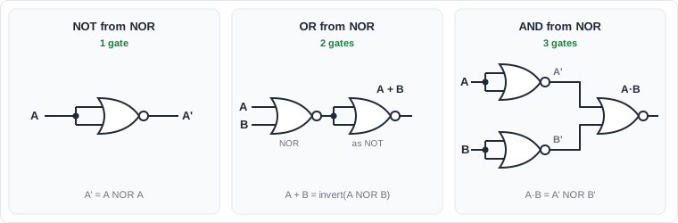
NOT :  A'     = A NOR A                           1 gate
OR  :  A + B  = (A NOR B) NOR (A NOR B)           2 gates  (NOR, then a NOR used as NOT)
AND :  A . B  = (A NOR A) NOR (B NOR B)           3 gates  (invert both inputs, then NOR)
The two families have mirror-image costs. Each is cheap for the function closest to it and needs extra inverters for the other:
| Function | 2-input NAND gates | 2-input NOR gates |
|---|---|---|
| NOT | 1 | 1 |
| AND | 2 | 3 |
| OR | 3 | 2 |
| XOR | 4 | 5 |
| XNOR | 5 | 4 |
The XOR and XNOR counts are minimums: an exhaustive search over all circuits of 2-input NAND gates finds no XOR with fewer than 4 gates and no XNOR with fewer than 5.
Converting a Function to NAND-Only Form
Take F = (A . B) + C'. The naive method is to replace every gate with its NAND equivalent from the table above:
Step 1  Replace each gate:
          A . B   -> 2 NANDs   (NAND + inverter)
          C'      -> 1 NAND    (inverter)
          X + Y   -> 3 NANDs   (two inverters + NAND)
        Total: 6 NAND gates

Step 2  Look for two inverters back to back. The AND's output inverter feeds
        the OR's input inverter, and the C' inverter feeds the other OR input
        inverter. NOT(NOT(x)) = x, so both pairs cancel.

Step 3  What remains:   F = (A NAND B) NAND C        2 NAND gates
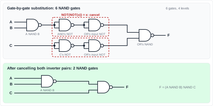
The reduced circuit passes every row of the truth table:
| A | B | C | A NAND B | (A NAND B) NAND C | AB + C' |
|---|---|---|---|---|---|
| 0 | 0 | 0 | 1 | 1 | 1 |
| 0 | 0 | 1 | 1 | 0 | 0 |
| 0 | 1 | 0 | 1 | 1 | 1 |
| 0 | 1 | 1 | 1 | 0 | 0 |
| 1 | 0 | 0 | 1 | 1 | 1 |
| 1 | 0 | 1 | 1 | 0 | 0 |
| 1 | 1 | 0 | 0 | 1 | 1 |
| 1 | 1 | 1 | 0 | 1 | 1 |
A faster route skips the naive step entirely. Any sum-of-products expression maps directly onto two levels of NAND gates:
Rule for SOP -> NAND-NAND
  1. Each product term becomes a first-level NAND of its literals.
  2. A single-literal term goes straight to the second level, inverted.
     (C' becomes plain C at the second-level input.)
  3. One second-level NAND combines everything.

F = A.B + C'   ->   first level: A NAND B        second level: (A NAND B) NAND C
The NOR-only version of the same function shows why the form of the expression matters. NOR gates map naturally onto product-of-sums form, so F is first rewritten as (A + C')(B + C'):
C'  = C NOR C                         1 gate
P   = A NOR C'                        1 gate   (P = (A + C')')
Q   = B NOR C'                        1 gate   (Q = (B + C')')
F   = P NOR Q                         1 gate   (F = (A + C')(B + C'))
Total: 4 NOR gates, against 2 NAND gates for the same function
Quick Check
Q: Convert F = A'B + C to NAND-only form. How many 2-input NAND gates does it take?
Show Answer
Four. The product A'B needs A' = A NAND A, then a first-level NAND: T = A' NAND B. The single literal C must arrive at the second level inverted, so C' = C NAND C. Finally F = T NAND C'. That is 4 gates, and an exhaustive search confirms no 3-gate circuit exists. If C' is already available elsewhere in the circuit, the count drops to 3.
XOR from Four NAND Gates
XOR is 1 when its inputs differ: A XOR B = A.B' + A'.B. A direct SOP conversion would need two inverters plus three NANDs, five gates in total. The classic four-gate circuit saves one by sharing the term T1 = A NAND B between both halves:
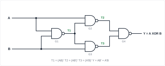
| A | B | T1 = A NAND B | T2 = A NAND T1 | T3 = B NAND T1 | Y = T2 NAND T3 |
|---|---|---|---|---|---|
| 0 | 0 | 1 | 1 | 1 | 0 |
| 0 | 1 | 1 | 1 | 0 | 1 |
| 1 | 0 | 1 | 0 | 1 | 1 |
| 1 | 1 | 0 | 1 | 1 | 0 |
Why it works: T1 equals (A.B)', so T2 = (A.(A.B)')' simplifies to (A.B')', and T3 simplifies to (A'.B)'. The final NAND turns these two inverted products into A.B' + A'.B. The same four-gate structure built from NOR gates produces XNOR instead of XOR.
Why Chip Libraries Lean on NAND
In static CMOS, every single-stage gate is inverting. A pull-down network of NMOS transistors pulls the output low, and a complementary pull-up network of PMOS transistors pulls it high. NAND, NOR, and NOT are therefore the natural one-stage gates. An AND gate in a cell library is really a NAND followed by an inverter: 6 transistors instead of 4, and two stages of delay instead of one.
NAND and NOR have the same transistor count, but not the same quality:
- A NAND gate puts its NMOS transistors in series and its PMOS transistors in parallel.
- A NOR gate puts its PMOS transistors in series and its NMOS transistors in parallel.
- Holes move about half as fast as electrons, so a PMOS transistor already needs to be roughly twice as wide as an NMOS to deliver the same current. Putting PMOS in series makes it worse: each one must be widened again to make up for the stack.
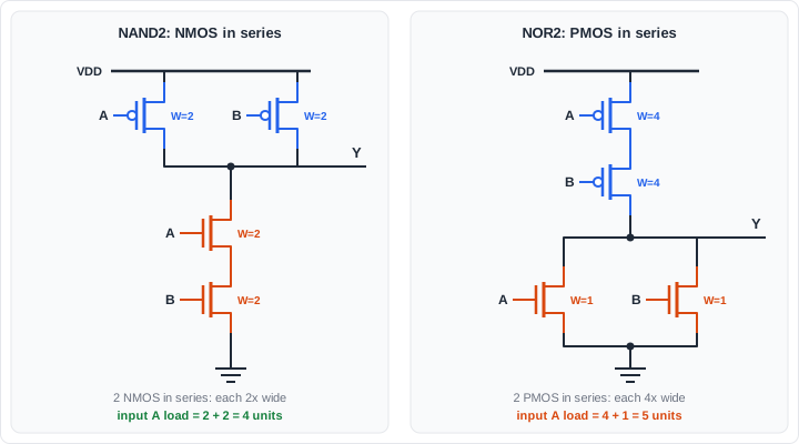
Sizing every gate to have the same drive strength as a reference inverter (NMOS width 1, PMOS width 2) gives these input capacitances. Higher input capacitance means a gate is a heavier load on whatever drives it, so it slows down the logic before it:
| Gate | NMOS width (each) | PMOS width (each) | Capacitance per input | Relative to inverter |
|---|---|---|---|---|
| Inverter | 1 | 2 | 3 | 1.00 |
| NAND2 | 2 | 2 | 4 | 1.33 |
| NOR2 | 1 | 4 | 5 | 1.67 |
| NAND3 | 3 | 2 | 5 | 1.67 |
| NOR3 | 1 | 6 | 7 | 2.33 |
| NAND4 | 4 | 2 | 6 | 2.00 |
| NOR4 | 1 | 8 | 9 | 3.00 |
A NOR4 costs as much input capacitance as a NAND4 plus half again, and it uses wide, slow PMOS stacks that take up area. That is why wide NOR gates are used sparingly, and why designers and synthesis tools favour NAND-based structures on fast paths.
Real libraries are not NAND-only. They contain NAND, NOR, AND, OR, XOR, and complex AND-OR-INVERT (AOI) and OR-AND-INVERT (OAI) cells in several drive strengths. NAND is simply the most efficient multi-input building block, so NAND cells and inverters are among the most heavily used cells in synthesized designs.
What Comes Out of Synthesis
Synthesis tools do not convert your logic to NAND-only form. They optimize the Boolean equations and then pick whichever library cells meet timing with the least area. Universal-gate thinking still predicts the result well:
You describe              Synthesis typically produces
-----------------------   -------------------------------------------------
A.B + C.D                 NAND2, NAND2 -> NAND2           (NAND-NAND, no inverters)
(A.B + C.D)'              one AOI22 cell                  (single inverting stage)
A.B (used by itself)      AND2 cell = NAND2 + inverter    (or the NAND2 alone if
                                                           the next gate can use
                                                           the inverted signal)
8-input AND               NAND4, NAND4 -> NOR2            (a tree; no 8-high stack)
The last row combines both families: two NAND4 gates produce (first half)' and (second half)', and a NOR2 of those two inverted signals is 1 only when both halves are all 1s.
Where Do Universal Gates Show Up?
- Breadboard logic: The classic 7400 chip holds four 2-input NAND gates. That is exactly enough to build one XOR, or one 2-to-1 multiplexer, from a single chip.
- Spaceflight computing: The Apollo Guidance Computer was built almost entirely from one kind of integrated circuit: a three-input NOR gate (one per chip in the early version, two per chip in the version flown on crewed missions). Using a single gate type simplified qualification and testing.
- Flash memory names: NAND flash gets its name from its memory cells, which sit in series strings like the NMOS stack of a NAND gate. The bit line is pulled low only when every cell in the string conducts. NOR flash connects each cell directly to the bit line, like the parallel NMOS of a NOR gate.
- Standard-cell ASICs: Synthesized logic is dominated by NAND2, NAND3, inverters, and AOI/OAI cells, all single-stage inverting gates.
FPGAs are different: they implement logic in look-up tables (LUTs), small memories that store a truth table directly. A LUT does not care whether your function is written with NANDs or ANDs; universal-gate conversions matter for custom chips and standard-cell flows, not for FPGA fabric.
Common Mistakes
Mistake #1: Swapping the NAND and NOR truth tables
NAND outputs 0 only when all inputs are 1. NOR outputs 1 only when all inputs are 0. A quick check: a NAND with any input at 0 always outputs 1; a NOR with any input at 1 always outputs 0.
Mistake #2: Grounding or floating the spare input of an inverter
To use a NAND as an inverter, tie both inputs together or tie the spare input to 1. Tying it to 0 forces the output to a constant 1. For a NOR, the spare input must go to 0. A floating CMOS input drifts to an undefined voltage and can turn both transistor networks partly on, causing wrong values and wasted current.
Mistake #3: Dropping an inversion
One NAND gate gives NAND, not AND: a second NAND used as an inverter is needed. Likewise, A NAND B is not A OR B; both inputs must be inverted first. When converting, count the bubbles on each path: an odd number means the signal is inverted.
Mistake #4: Treating NAND as associative
AND is associative, NAND is not. Chaining two 2-input NANDs gives (A NAND B) NAND C = A.B + C', which differs from a 3-input NAND in four of the eight input rows. To build NAND3 from 2-input gates, AND two inputs first (two NANDs), then NAND the result with the third input.
Mistake #5: Stopping after gate-by-gate substitution
Replacing each AND, OR, and NOT with its NAND equivalent works, but leaves pairs of back-to-back inverters. In the worked example these inflate a 2-gate circuit to 6 gates. Always cancel double inversions, or use the SOP to NAND-NAND rule directly.
Practice Exercise
Challenge: Design a 2-to-1 Multiplexer Using Only NAND Gates
A 2-to-1 multiplexer outputs A when the select input S is 0 and B when S is 1: Y = S'.A + S.B.
- Build Y using only 2-input NAND gates. How many gates do you need?
- How many transistors does your circuit use in CMOS?
- Verify your circuit for all eight combinations of S, A, and B.
Hint
Y is already in SOP form with two product terms. Apply the SOP to NAND-NAND rule, and remember that S' must be generated.
Solution
1. S'  = S NAND S             (inverter)
   T1  = S' NAND A            (first-level NAND for S'.A)
   T2  = S NAND B             (first-level NAND for S.B)
   Y   = T1 NAND T2           (second level)
   Total: 4 NAND gates. An exhaustive search confirms 4 is the minimum.

2. 4 gates x 4 transistors = 16 transistors.

3. S A B | S' T1 T2 | Y
   0 0 0 |  1  1  1 | 0   (Y = A = 0)
   0 0 1 |  1  1  1 | 0   (Y = A = 0)
   0 1 0 |  1  0  1 | 1   (Y = A = 1)
   0 1 1 |  1  0  1 | 1   (Y = A = 1)
   1 0 0 |  0  1  1 | 0   (Y = B = 0)
   1 0 1 |  0  1  0 | 1   (Y = B = 1)
   1 1 0 |  0  1  1 | 0   (Y = B = 0)
   1 1 1 |  0  1  0 | 1   (Y = B = 1)

The same 4 gates fit in one quad 2-input NAND chip.
Summary
In this tutorial, you learned:
- NAND and NOR are universal because they can build NOT, AND, and OR; AND and OR alone cannot invert
- NOT takes 1 gate in either family; AND takes 2 NANDs or 3 NORs; OR takes 3 NANDs or 2 NORs
- XOR takes a minimum of 4 NAND gates, and the same structure in NOR gives XNOR
- SOP expressions map directly to NAND-NAND, and POS expressions map to NOR-NOR; always cancel back-to-back inverters
- NAND is not associative: chained 2-input NANDs do not make a wider NAND
- CMOS gates are naturally inverting, and NAND's series NMOS stack is cheaper than NOR's series PMOS stack, so libraries and synthesis results lean on NAND
