
Every gate input connected to a net is a small capacitor that the net's driver must charge and discharge. Fanout is the number of inputs a driver feeds, and loading is the total capacitance it sees: all those input pins plus the wire joining them. More load means slower edges and more delay. When one signal must reach many destinations, the standard fix is to split the load with a tree of buffers.
12 min read | Intermediate Level
What You'll Learn
- How fanout and wire capacitance add up to a driver's load
- How load affects delay and transition time
- How buffer chains are sized, and how buffer trees and register duplication handle high-fanout nets
- Which design rules limit fanout, and how implementation tools enforce them
What a Driver Sees
Load on a net

  total load  =  sum of input pin capacitances of every receiver
               + wire capacitance of the net

  more receivers      -> more pin capacitance
  receivers far apart -> longer net -> more wire capacitance
  larger receiver cells (X4, X8) -> larger input capacitance per pin
The delay of the driving gate has two parts: a fixed part from its own internal capacitance, and a part proportional to its load. Doubling the load roughly doubles the load-dependent part. The output transition time (slew) also grows with load, and a slow edge makes every receiving gate slower and burns more short-circuit power in it.
Driver delay in proportions (illustrative numbers)

  delay = intrinsic delay + (drive resistance x load)
        = 15 ps          + 3 ps per fF of load

  fanout 4  (4 x 1.7 fF  =  6.8 fF)  ->  15 + 20  =  35 ps
  fanout 8  (8 x 1.7 fF  = 13.6 fF)  ->  15 + 41  =  56 ps
  fanout 32 (32 x 1.7 fF = 54.4 fF)  ->  15 + 163 = 178 ps
Quick Check
Q: A driver's load doubles. Does its delay double?
Show Answer
Not exactly. Only the load-dependent part doubles; the intrinsic part stays the same. For a heavily loaded driver the delay nearly doubles; for a lightly loaded one it rises less.
High-Fanout Nets and Buffer Trees
Some signals naturally reach hundreds or thousands of destinations: resets, enables, scan-enable, mux selects in wide datapaths, and clocks. No single cell can drive that directly. The load is split into a tree of buffers so that each buffer drives a moderate load:
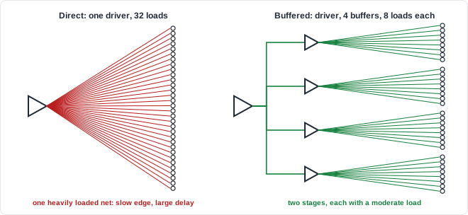
Direct vs. buffered, using the illustrative numbers above

  Direct: one driver, 32 loads                -> 178 ps, very slow edge

  Buffered: driver -> 4 buffers -> 8 loads each
    stage 1: driver sees 4 buffer inputs (3 fF each) + wire = 12.8 fF
             15 + 3 x 12.8                                    =  53 ps
    stage 2: each buffer (stronger: 1.5 ps/fF) sees 8 loads = 13.6 fF
             15 + 1.5 x 13.6                                  =  35 ps
    total                                                     = ~88 ps
Adding a stage made the net about twice as fast, because neither stage is badly overloaded. The same principle as a tapered buffer chain applies: keep the fanout of each stage moderate.
How Many Stages? The Rule of Four
The buffer tree above used a fixed fanout. The general question is: when a small gate must drive a load much bigger than its own input, how many buffer stages are best? Let F be the ratio of the final load capacitance to the first gate's input capacitance. One stage driving the whole load has a delay proportional to F. Splitting the job into N stages makes each stage drive only F1/N times its own input, but each stage adds its own fixed delay. Working through the trade-off, the delay is smallest when each stage drives about four times its own input, which is why the fanout-of-4 inverter is the standard yardstick for delay.
| Load ratio F | Best number of stages N = log4 F | Fanout of each stage |
|---|---|---|
| 4 | 1 | 4 |
| 16 | 2 | 4 |
| 64 | 3 | 4 |
| 256 | 4 | 4 |
Take F = 64: one stage would have a normalized delay of about 65 (64 + 1 fixed), while three stages of fanout 4 each have a delay of 3 × (4 + 1) = 15, over four times faster. The optimum is flat: a larger fanout per stage costs only a little extra delay and saves a lot of transistor size, so buffers that drive pads or long wires often use a fanout of 8 to 12 per stage. Clock and reset buffer trees follow the same rule (see also Gate Sizing & Drive Strength).
Where Do High-Fanout Nets Appear?
A global reset or a scan-enable signal can fan out to every flip-flop in a block - hundreds of thousands of loads. Write enables and select lines in wide memories and datapaths fan out to every bit slice. Implementation tools build dedicated buffer trees for these nets, and clocks get the most careful treatment of all through clock tree synthesis.
How Tools Handle High-Fanout Nets
During logic synthesis, very high-fanout nets such as reset and scan-enable are often treated as ideal (no delay) on purpose, because their buffering depends on placement. Physical implementation then builds the buffer trees. Libraries and flows define design rules that every net must meet:
| Design rule | Limits | Why it exists |
|---|---|---|
| Max fanout | Number of pins on a net | Keeps loads reasonable before exact capacitance is known |
| Max capacitance | Total load on an output pin | Stays within the range the cell was characterized for |
| Max transition | Slowest allowed edge on a net | Protects timing accuracy, noise immunity, and power |
The exact limits vary by library and design, but the tools fix violations the same way: upsize the driver, insert buffers, or split the net.
Design Technique: Register Duplication
When a single flip-flop drives a very large fanout on a critical path, splitting the load at the source helps: duplicate the register so that each copy drives part of the load.
One enable register driving 256 datapath bits is a heavily loaded net

  before:  [EN] ------------------------> 256 bits          load = 256 pins

  after :  [EN_LO] ---------------------> bits 0..127       load = 128 pins
           [EN_HI] ---------------------> bits 128..255     load = 128 pins
           both registers are loaded with the same value at every clock edge
Tool note: because the two copies are logically identical, synthesis may merge them back into one register unless told to keep them. Tools provide attributes or settings to preserve duplicates, and many can perform register duplication automatically during timing optimization, which is usually the better choice.
Common Mistakes
Mistake #1: Counting only the number of loads
Fanout count is a rough guide. What the driver really sees is capacitance: pin capacitance (which varies with cell size) plus wire capacitance (which grows with distance). Ten loads spread across a block can be heavier than thirty loads packed together.
Mistake #2: Driving a huge load with one very large cell
A giant driver presents a giant input capacitance to whatever drives it, moving the problem back one stage. A buffer tree spreads the load so that no stage is overloaded.
Mistake #3: Treating ideal nets in synthesis as final
Reset and scan-enable nets marked ideal in synthesis have zero delay only on paper. After buffering, they have real insertion delay and skew, which matters for reset release timing and must be checked after implementation.
Mistake #4: Expecting duplicated registers to survive automatically
Logically identical registers are prime candidates for merging during optimization. Without the tool-specific setting to preserve them, duplicates made by hand may disappear from the netlist.
Practice Exercise
Challenge: Buffer a 64-Load Net
Use the illustrative model: a driver or X1 buffer has delay 15 ps + 3 ps per fF; an X2 buffer has 15 ps + 1.5 ps per fF and an input capacitance of 3 fF. Each load pin is 1.5 fF, and each pin adds 0.2 fF of wire.
- Estimate the delay of the driver driving all 64 loads directly.
- Estimate the delay with the driver feeding 8 X2 buffers, each driving 8 loads.
Hint
Each load costs 1.5 + 0.2 = 1.7 fF. Each buffer input costs 3 + 0.2 = 3.2 fF.
Solution
1. Direct: 64 x 1.7 fF = 108.8 fF
   delay = 15 + 3 x 108.8 = ~341 ps

2. Stage 1: 8 buffers x 3.2 fF = 25.6 fF -> 15 + 3 x 25.6   = ~92 ps
   Stage 2: 8 loads x 1.7 fF   = 13.6 fF -> 15 + 1.5 x 13.6 = ~35 ps
   Total                                                     = ~127 ps

   The buffered net is about 2.7x faster, and its edges are much sharper.
Summary
In this tutorial, you learned:
- A driver's load is the sum of its receivers' pin capacitances plus the wire capacitance
- Delay has a fixed intrinsic part plus a part proportional to load; transition time also grows with load
- High-fanout nets are split into buffer trees so that each stage drives a moderate load
- Max fanout, max capacitance, and max transition rules are enforced during implementation
- Reset and scan-enable nets are often ideal in synthesis and buffered later
- Each buffer stage should drive about four times its own input capacitance; a load ratio F needs about log4 F stages
- Register duplication splits load at the source, but duplicates must be protected from merging
