
The RTL-to-GDSII flow is the sequence of steps that turns a register-transfer-level (RTL) description of a design into the polygon database a foundry manufactures. Logic synthesis converts RTL into a netlist of standard cells. Physical design places those cells on the die, builds the clock tree, and routes the wires. Sign-off checks timing with real wire parasitics and verifies the layout against manufacturing rules and the original netlist. The final output is a GDSII file, and handing it to the foundry is called tape-out.
15 min read | Intermediate Level
What You'll Learn
- The main steps from RTL to GDSII and what each one produces
- What a synthesized netlist and a timing constraint file look like
- Which checks at each stage catch which kinds of problems
- How RTL decisions show up later in the physical flow
The Flow at a Glance
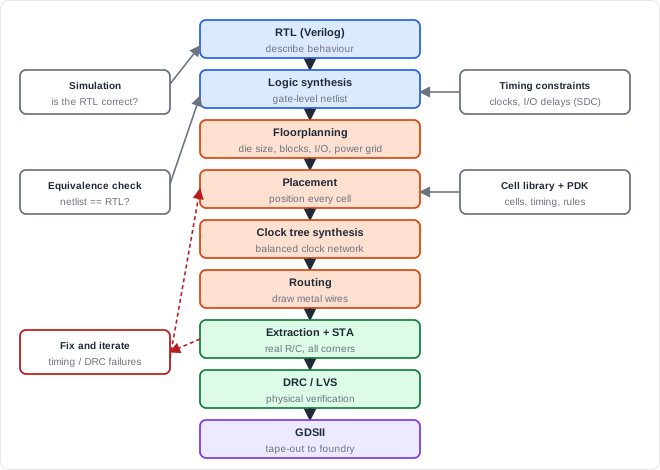
| Step | Input | Output | Main question answered |
|---|---|---|---|
| RTL design + simulation | Specification | Verified RTL | Does the design do the right thing? |
| Logic synthesis | RTL, timing constraints, cell library | Gate-level netlist | Which cells implement this logic, fast and small enough? |
| Floorplanning | Netlist, die size target | Die outline, block and macro positions, I/O, power grid | Where does everything go at a high level? |
| Placement | Floorplan, netlist | A legal position for every cell | Can connected cells sit close together without congestion? |
| Clock tree synthesis | Placed design | Buffered, balanced clock network | Does the clock reach every flop with small skew? |
| Routing | Placed design with clock tree | Metal wires and vias for every net | Can every connection be drawn within the rules? |
| Extraction + static timing analysis | Routed layout | Timing reports at all corners | Does every path meet setup and hold with real wires? |
| Physical verification | Final layout | DRC and LVS results | Can it be manufactured, and does it match the netlist? |
| Tape-out | Clean layout | GDSII (or OASIS) database | Ready for mask making |
Front End: From RTL to Netlist
Synthesis reads RTL plus a constraint file that describes clocks and I/O timing. Without constraints, synthesis has no timing target and paths are left unchecked.
| Constraint | Example | What it tells the tools |
|---|---|---|
| Clock definition | 1 GHz clock (1 ns period) | The required time for every register-to-register path |
| Clock uncertainty | 50 ps | Margin for jitter and supply noise |
| Input delay | 300 ps after the clock edge | How late each input arrives from outside |
| Output delay | 300 ps before the next edge | How much time the outside logic needs |
The result is a gate-level netlist: a list made only of cell instances from the library and the wires connecting them.
Design function (RTL):   Y = (A . B) + C

Synthesized netlist (illustrative cell and pin names; every library uses its own):
  U1 : AOI21_X1   inputs A1 = A, A2 = B, B = C     output N1 = NOT((A . B) + C)
  U2 : INV_X1     input  A  = N1                   output Y  = NOT N1
An equivalence check then proves mathematically that the netlist performs the same function as the RTL, without simulation vectors. It is repeated after every major netlist change in the physical flow.
Quick Check
Q: Synthesis finishes with no timing violations, but the design has no clock-definition constraint. Is timing safe?
Show Answer
No. Without a clock definition, register-to-register paths have no required time, so they are unconstrained and never reported as failing. "No violations" means nothing was checked. Always review the report of unconstrained paths.
Back End: Physical Design
Physical design, step by step (simplified)

  Floorplan   : choose die size; place large macros (SRAMs, analog, I/O);
                build the power grid (rings, stripes, rails)
  Placement   : put every standard cell in a legal row position;
                optimize wire length and timing; avoid congested areas
  CTS         : build the clock tree; fix hold violations it reveals
  Routing     : draw every wire on the metal layers, obeying spacing and width rules
  Optimize    : resize cells, insert buffers, fix timing and design-rule violations
                (small netlist edits here are called ECOs - engineering change orders)
  Fill        : add filler cells and metal fill for manufacturing uniformity
Where Does the Back End Take the Most Time?
For a large SoC, the physical flow is iterative and often takes longer than writing the RTL. Timing closure - repeatedly finding failing paths and fixing them by resizing, buffering, moving cells, or changing RTL - can take many weeks. Large designs are split into hierarchical blocks, each placed and routed separately and then assembled at the top level.
Sign-Off: Timing and Physical Verification
| Check | What it verifies | Typical failures |
|---|---|---|
| Static timing analysis (multi-corner) | Setup and hold on every path at every process, voltage, and temperature corner, with extracted parasitics and crosstalk | Long paths, hold violations after CTS, crosstalk delay |
| IR drop and electromigration | Supply voltage at every cell; current density in wires | Weak power grid, hot spots |
| DRC (design rule check) | Every shape obeys the foundry's width, spacing, enclosure, and density rules | Spacing violations, missing fill |
| LVS (layout vs. schematic) | The layout's connectivity matches the netlist exactly | Shorts, opens, missing connections |
| Antenna and other checks | Manufacturing-induced damage risks, such as long wires charging gate oxides during etching | Long unprotected wires on thin gates |
Only when every check is clean at every corner does the design tape out: the final layout is written as a GDSII (or the newer OASIS) file and sent to the foundry, which uses it to make the photomasks.
Where Do Flow Mistakes Get Expensive?
A mask set for an advanced process is very expensive, and a manufacturing cycle takes months. A bug that escapes sign-off can force a re-spin: new masks and another fabrication run. This is why teams invest heavily in verification before tape-out, and why sign-off checks are run on the exact final database.
How RTL Decisions Show Up Later
| RTL decision | Where it shows up in the flow |
|---|---|
| Deep combinational logic between registers | Timing closure struggles in placement and STA |
| Signals that must cross the die in one cycle | Unfixable wire delay after placement |
| High-fanout controls from a single flop | Large buffer trees, extra delay and power |
| Gated or generated clocks built from logic | Difficult CTS, extra constraints, glitch risk |
| Large memories written as arrays | Huge flip-flop-based storage unless replaced with SRAM macros |
| Unintended latches from combinational logic that leaves an output unspecified for some inputs | Unexpected latches in the netlist, timing-analysis complications |
Common Mistakes
Mistake #1: Treating post-synthesis timing as final
Synthesis only estimates wire delay. Real wire lengths, clock-tree latency, and crosstalk appear after placement and routing. Timing is only closed when it passes with extracted parasitics at all corners.
Mistake #2: Missing or incomplete constraints
Paths without constraints are not timed and cannot fail, which hides real problems. Every clock, generated clock, and I/O must be constrained, and the unconstrained-path report should be empty or fully explained.
Mistake #3: Ignoring synthesis warnings
Inferred latches, multiple drivers, and undriven nets usually mean the RTL does not describe the intended hardware. Simulation may still pass while the netlist behaves differently. Review and clear synthesis warnings before moving on.
Mistake #4: Skipping equivalence checks after netlist changes
Every optimization and ECO modifies the netlist. Without an equivalence check against the RTL, a functional change introduced during implementation can reach silicon.
Practice Exercise
Challenge: Which Step Catches It?
For each problem, name the step or check most likely to catch it first:
- An FSM goes to the wrong state for one input sequence.
- A combinational logic description leaves an output unspecified for some input combinations.
- A 4 mm route between two blocks has negative setup slack.
- Two metal wires are drawn too close together.
- A buffer inserted during optimization accidentally connects to the wrong net.
Hint
Think about what each check compares: behaviour against intent, netlist against RTL, timing against constraints, layout against rules, or layout against netlist.
Solution
1. RTL simulation (functional verification)
2. Synthesis warnings: an inferred latch
3. Post-placement / post-route static timing analysis with extracted wires
4. DRC (design rule check)
5. Equivalence checking (netlist vs. RTL); LVS would also catch a layout
   that does not match its netlist
Summary
In this tutorial, you learned:
- Logic synthesis turns RTL and constraints into a gate-level netlist of library cells
- Floorplanning, placement, clock tree synthesis, and routing turn the netlist into a layout
- Static timing analysis with extracted parasitics, at every corner, decides whether timing is met
- DRC checks manufacturability; LVS checks that the layout matches the netlist
- Equivalence checking proves that netlists still match the RTL after every change
- The final GDSII database goes to the foundry at tape-out
- RTL choices such as logic depth, clocking, and memory style strongly affect every later step
