
A sum-of-products (SOP) expression maps directly onto a two-level NAND-NAND network, and a product-of-sums (POS) expression maps onto a two-level NOR-NOR network. In static CMOS, NAND gates are faster and smaller than NOR gates, so SOP-style NAND structures are the usual choice. In practice, synthesis tools use SOP and POS only as starting points: they factor the logic into multiple levels and map it onto whatever library cells - NAND, NOR, AOI, OAI - give the best timing and area.
12 min read | Intermediate Level
What You'll Learn
- Why AND-OR equals NAND-NAND and OR-AND equals NOR-NOR
- How to decide whether SOP or POS gives the smaller circuit
- Why CMOS favours NAND-based implementations
- How synthesis turns Boolean expressions into library cells
From Two-Level Logic to Gates
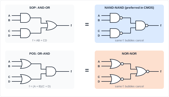
The equivalence comes from De Morgan's theorem. Replace every gate in an AND-OR network with a NAND: the bubble at each first-level output cancels the bubble at the second-level input, and a NAND with inverted inputs is an OR.
Bubble pushing: why AND-OR = NAND-NAND

  f = AB + CD
    = NOT( NOT(AB + CD) )                  double negation
    = NOT( NOT(AB) AND NOT(CD) )           De Morgan
    = NAND( NAND(A,B), NAND(C,D) )         two levels of NAND

  f = (A + B)(C + D)
    = NOT( NOT(A + B) OR NOT(C + D) )      De Morgan
    = NOR( NOR(A,B), NOR(C,D) )            two levels of NOR
The same rule works for any number of product or sum terms: an SOP with k products becomes k first-level NAND gates feeding one k-input NAND; a POS with k sums becomes k first-level NOR gates feeding one k-input NOR.
If a product or sum term uses a complemented literal such as NOT A, that complement must come from somewhere: an inverter, or the inverted output (QN) of a flip-flop. Complemented literals add inverters and one more level of delay to a two-level circuit.
Why CMOS Prefers NAND-NAND
A two-level NAND-NAND circuit stacks NMOS transistors in series and puts PMOS in parallel. A NOR-NOR circuit stacks PMOS in series. Because PMOS devices are slower, series PMOS stacks must be made much wider to keep up.
| Implementation | Series stack in each gate | Logical effort (2-input gate) | Typical choice |
|---|---|---|---|
| SOP as NAND-NAND | NMOS (fast) | 4/3 | Preferred in static CMOS |
| POS as NOR-NOR | PMOS (slow) | 5/3 | Used when POS is much smaller |
The preference flips in some other circuit styles. Dynamic logic and older pseudo-NMOS logic pull down through NMOS only, so NOR (parallel NMOS) is their fast gate. That is why classic PLAs (programmable logic arrays) build their AND and OR planes as NOR-NOR structures, with inverters on the inputs and outputs to produce SOP logic.
SOP or POS: Which Is Smaller?
Minimize the function both ways and compare. A useful rule of thumb: if the function has few 1s, SOP tends to be smaller; if it has few 0s, POS tends to be smaller.
Worked example: f = 1 when (A or B) is true AND (C or D) is true

  Minimal POS:  f = (A + B)(C + D)                 2 sums,     4 literals
  Minimal SOP:  f = AC + AD + BC + BD              4 products, 8 literals

  Two-level cost in transistors:
    SOP, NAND-NAND : 4 x NAND2 (16) + NAND4 (8)   = 24 transistors, 2 levels
    POS, NOR-NOR   : 2 x NOR2  (8)  + NOR2  (4)   = 12 transistors, 2 levels
    Complex gate   : OAI22 (8) + inverter (2)     = 10 transistors
Here POS is clearly better, and a complex OAI gate is better still. The minimal two-level form is not the end of the story: factoring, as in (A + B)(C + D), often beats both flat forms.
Quick Check
Q: A 4-input function is 1 for 14 of its 16 input combinations. Would you start from its SOP or its POS form?
Show Answer
POS. With only two 0s, the POS form needs at most two sum terms, while the SOP form must cover fourteen 1s and usually needs several product terms.
What Synthesis Actually Does
Synthesis tools do not build your expression literally. They convert it to an internal Boolean network, optimize it, and then map it onto the cells in the target library:
Logic synthesis, simplified

  1. Parse the logic description into a technology-independent Boolean network
  2. Optimize the network:
       two-level minimization of each node (SOP/POS)
       factoring and sharing: AC + AD + BC + BD -> (A + B)(C + D)
       don't-care exploitation
  3. Technology mapping: cover the network with library cells
       (NAND, NOR, AOI, OAI, MUX, XOR ...) minimizing delay on critical
       paths and area elsewhere
  4. Timing-driven restructuring and gate sizing
Two descriptions of the same function

  Sum of products :  f = AC + AD + BC + BD
  Product of sums :  f = (A + B)(C + D)

  Both typically map to the same cells, for example an OAI22 followed by an
  inverter, or a single OA22 cell if the library provides one.
  The way the expression is written does not fix the gate structure.
Where Do Two-Level Forms Still Appear?
Instruction decoders, control-signal generators, and state-machine output logic are often described as truth tables, which are naturally SOP. Synthesis minimizes them as two-level functions before factoring. Programmable logic such as CPLDs still uses a product-term (SOP) architecture, so the number of product terms decides whether a function fits in one macrocell.
Where Does the Choice Stop Mattering?
In FPGAs, logic is implemented in look-up tables (LUTs). Any function of up to the LUT's input count - typically 4 to 6 inputs - costs one LUT regardless of whether its SOP or POS form is larger. SOP-versus-POS cost matters for ASIC standard-cell mapping, not for small FPGA functions.
Common Mistakes
Mistake #1: Believing the written form decides the gate structure
Writing an expression as SOP does not produce a NAND-NAND circuit, and writing it as POS does not produce NOR-NOR. Synthesis normalizes the logic and chooses cells for timing and area. Write the clearest expression and let the tool optimize.
Mistake #2: Assuming the minimal SOP is the minimal circuit
Minimal SOP minimizes a two-level implementation. Multi-level factoring, shared subexpressions, and complex AOI/OAI cells frequently produce smaller and faster circuits than any flat SOP or POS form.
Mistake #3: Swapping only some gates when converting to NAND-NAND
The AND-OR to NAND-NAND conversion works because the bubbles cancel in pairs. Replacing only the first-level gates, or only the output gate, leaves unpaired inversions and computes a different function. Convert both levels together, or push bubbles carefully through every wire.
Mistake #4: Ignoring the cost of complemented literals
A term such as A·NOT B needs an inverter on B. In two-level cost comparisons, count the inverters: they add transistors and an extra gate delay, and they can change which form is actually smaller.
Practice Exercise
Challenge: Not-All-Equal Detector
f(A, B, C) = 1 unless A = B = C (that is, f = 0 only for 000 and 111).
- Write the minimal POS and a minimal SOP.
- Count transistors for a NOR-NOR POS implementation and a NAND-NAND SOP implementation, including three inverters for complemented literals in each.
- Which would you expect to be faster, and why?
Hint
Each 0 gives one sum term in POS. For SOP, the six 1-cells can be covered by three 2-literal products.
Solution
1. POS: f = (A + B + C)(A' + B' + C')
   SOP: f = A'C + AB' + BC'   (covers 001,011 / 100,101 / 010,110)

2. POS NOR-NOR : 2 x NOR3 (12) + NOR2 (4) + 3 inverters (6) = 22
   SOP NAND-NAND: 3 x NAND2 (12) + NAND3 (6) + 3 inverters (6) = 24

3. The SOP version is likely faster despite being slightly larger.
   The POS version uses NOR3 gates with three PMOS in series (logical
   effort 7/3), while the SOP version uses NAND2 and NAND3 gates whose
   series stacks are fast NMOS (logical effort 4/3 and 5/3).
The same function can also be written as f = (A xor B) + (B xor C); the synthesis tool picks the gate structure either way.
Summary
In this tutorial, you learned:
- SOP (AND-OR) is equivalent to NAND-NAND, and POS (OR-AND) is equivalent to NOR-NOR, by De Morgan's theorem
- Static CMOS prefers NAND-NAND because it stacks fast NMOS transistors in series
- Choose the form with fewer terms: few 1s favour SOP, few 0s favour POS
- Factored forms and complex AOI/OAI cells often beat both flat two-level forms
- Synthesis optimizes and maps logic onto library cells; the way the expression is written does not fix the gate structure
- In FPGAs, small functions cost one LUT regardless of their SOP or POS size