
Logic HIGH and LOW are not exact voltages; they are ranges. A driver guarantees its output stays inside a valid range, and a receiver guarantees it will read any input inside a slightly wider range correctly. The gap between the two is the noise margin: how much noise can be added to a signal before the receiver might misread it. As supply voltages drop, those gaps shrink, which is why power-supply noise and crosstalk matter more in every new process.
12 min read | Intermediate Level
What You'll Learn
- What VOH, VOL, VIH, and VIL mean, and how they define the noise margins
- Where the input thresholds come from on a gate's transfer curve
- Which on-chip noise sources eat into the margins
- How voltage domains and I/O standards handle mismatched levels
Four Voltages, Two Margins
| Symbol | Meaning | Guaranteed by |
|---|---|---|
| VOH (min) | Lowest voltage a driver outputs for a HIGH | Driver |
| VOL (max) | Highest voltage a driver outputs for a LOW | Driver |
| VIH (min) | Lowest input voltage the receiver still reads as HIGH | Receiver |
| VIL (max) | Highest input voltage the receiver still reads as LOW | Receiver |
Noise margins

  NM_H (high)  =  VOH(min)  -  VIH(min)     noise that can pull a HIGH down safely
  NM_L (low)   =  VIL(max)  -  VOL(max)     noise that can push a LOW up safely

  Inputs between VIL and VIH are UNDEFINED: the receiver may read either value,
  or burn extra current while its output sits in the middle.
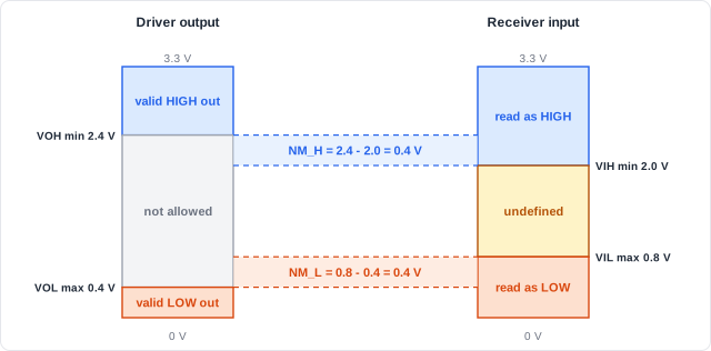
For the 3.3 V LVCMOS levels shown, the driver guarantees HIGH ≥ 2.4 V and LOW ≤ 0.4 V, and the receiver reads ≥ 2.0 V as HIGH and ≤ 0.8 V as LOW. Both margins are 0.4 V.
Where VIL and VIH Come From
A receiver's input thresholds come from its voltage transfer curve. VIL and VIH are usually defined at the two points where the curve's slope is -1, the unity-gain points. Between them, the gate has a gain greater than 1: small input changes cause large output changes, so input noise is amplified. Outside them, noise is attenuated.
That gain is what makes digital logic robust. A slightly degraded input produces a cleaner output, so every gate regenerates the signal. A chain of CMOS gates keeps restoring full logic levels, as long as each input stays outside the undefined region.
On-chip CMOS example (illustrative, VDD = 0.8 V)

  outputs swing almost rail to rail:  VOH ~ 0.8 V,  VOL ~ 0.0 V
  receiver thresholds:                VIL ~ 0.33 V, VIH ~ 0.47 V

  NM_L ~ 0.33 - 0.0 = 0.33 V
  NM_H ~ 0.8 - 0.47 = 0.33 V

  Same design at VDD = 1.2 V: margins scale up to roughly 0.5 V.
  Lower VDD -> smaller margins in absolute millivolts.
Quick Check
Q: A driver guarantees VOH ≥ 1.6 V and VOL ≤ 0.2 V. The receiver has VIH = 1.2 V and VIL = 0.6 V. What are the noise margins?
Show Answer
NM_H = 1.6 - 1.2 = 0.4 V. NM_L = 0.6 - 0.2 = 0.4 V.
What Eats the Margin On Chip
The margin is a budget, and several noise sources spend it at the same time:
| Noise source | Effect on a signal | Covered in more depth |
|---|---|---|
| IR drop and ground bounce | Driver and receiver see different local VDD and GND, so a "clean" HIGH or LOW is offset | Power/ground integrity |
| Crosstalk | A switching neighbour couples a glitch onto a quiet wire | Crosstalk and signal coupling |
| Supply ripple | The whole supply wobbles with switching activity | Power delivery design |
| Weak drivers (e.g. NMOS passing a 1) | The output never reaches the full rail | Transistor sizing and pass logic |
Margin budget check (illustrative, VDD = 0.8 V, NM_L = 0.33 V)

  ground bounce at the receiver       60 mV
  crosstalk glitch from a neighbour  120 mV
  driver VOL offset (IR drop)         40 mV
  --------------------------------------------
  worst-case total noise             220 mV   < 330 mV   -> safe, 110 mV to spare

  The same noise at VDD = 0.6 V (NM_L ~ 0.25 V) leaves only 30 mV.
Where Do Shrinking Margins Show Up?
Low-voltage mobile processors run parts of the chip at supplies well under 1 V to save power. At those levels, the same millivolts of supply noise or crosstalk consume a much larger fraction of the margin, so power-grid design, decoupling capacitance, and signal-integrity analysis are all tightened. Sign-off flows check glitch noise against each receiving cell's noise immunity, not just against timing.
Crossing Voltage Levels: Domains and I/O Standards
Noise margins also decide whether two circuits can be connected at all. A driver's guaranteed levels must fall inside the receiver's valid input ranges.
- Between on-chip voltage domains: a signal from a 0.6 V domain may not reliably drive a HIGH in a 0.9 V domain, and a low-voltage receiver driven from a higher domain can see its PMOS left partly ON. Level shifter cells are inserted at domain boundaries. They are described in the design's power intent, not in RTL, and implementation tools insert and verify them.
- At chip I/O: pads follow published interface standards (for example LVCMOS at 3.3 V, 2.5 V, or 1.8 V). Mixing standards without checking levels is a classic board-level bug.
- Noisy or slow inputs: input pads often include a Schmitt trigger, which uses two different thresholds for rising and falling inputs (hysteresis), so a slowly changing or noisy signal cannot toggle the output back and forth.
Where Are Small-Swing Interfaces Used?
High-speed memory and serial interfaces use small voltage swings to save power and switch faster. Instead of fixed thresholds, they compare the input against a reference voltage, or use differential signalling, where the receiver looks at the difference between two wires. Noise that hits both wires equally cancels out, giving good noise immunity despite the small swing.
Common Mistakes
Mistake #1: Treating the logic threshold as a single voltage
Receivers have two thresholds, VIL and VIH, with an undefined region between them. Designing to a single "switching point" ignores the region where the input is not guaranteed to be read correctly.
Mistake #2: Using nominal supply and ideal output levels
Margins must be computed with guaranteed worst-case levels at the lowest supply and worst temperature, not with typical values. A margin that looks comfortable at nominal conditions can vanish at the corners.
Mistake #3: Checking each noise source against the full margin separately
IR drop, ground bounce, and crosstalk can all happen at the same instant. They must fit in the margin together. Each passing individually proves nothing about the combination.
Mistake #4: Connecting different voltage domains directly
A signal from a lower-voltage domain may not reach the receiving domain's VIH, and it can leave the receiver drawing static current. Every crossing between domains needs a level shifter (and, if a domain can be powered off, isolation).
Practice Exercise
Challenge: Can a 1.8 V Driver Talk to a 3.3 V Receiver?
A 1.8 V driver guarantees VOH ≥ 1.35 V and VOL ≤ 0.45 V. A 3.3 V LVCMOS receiver has VIH = 2.0 V and VIL = 0.8 V.
- Compute NM_H and NM_L.
- Will the interface work? If not, what is needed?
Hint
A negative noise margin means the driver's guaranteed level does not reach the receiver's threshold even with zero noise.
Solution
1. NM_H = VOH - VIH = 1.35 - 2.0  = -0.65 V   (negative!)
   NM_L = VIL - VOL = 0.8  - 0.45 = +0.35 V

2. No. A HIGH from the driver can be as low as 1.35 V, which is
   inside the receiver's undefined region, even with no noise at all.
   The LOW works; the HIGH does not.
   Fix: a level shifter (or a receiver that supports 1.8 V levels).
Summary
In this tutorial, you learned:
- Logic levels are ranges: drivers guarantee VOH and VOL, receivers guarantee VIH and VIL
- NM_H = VOH - VIH and NM_L = VIL - VOL; inputs between VIL and VIH are undefined
- VIL and VIH sit at the unity-gain points of the transfer curve, and gain above 1 lets gates regenerate signals
- IR drop, ground bounce, crosstalk, and supply ripple all spend the same margin at once
- Lower supply voltages shrink noise margins in absolute terms
- Level shifters, I/O standards, Schmitt triggers, and differential signalling handle level mismatches and noise
