
A static RAM (SRAM) bit is stored in a tiny latch: two cross-coupled inverters that hold each other in one of two stable states. Two access transistors connect the latch to a pair of bit lines when the word line is raised. That makes six transistors per bit - the 6T SRAM cell. It is fast and needs no refresh, which is why caches, register files, and on-chip buffers are built from it. Its transistors must be sized carefully so that reading does not flip the stored bit, yet writing still can.
14 min read | Intermediate Level
What You'll Learn
- How a 6T SRAM cell stores, reads, and writes one bit
- Why read stability and writeability pull transistor sizing in opposite directions
- How SRAM arrays are organized with word lines, bit lines, and sense amplifiers
- How memories are built in a real chip: flip-flop arrays, memory-compiler macros, and FPGA block RAM
The 6T Cell
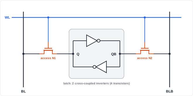
The two inverters form a loop: Q drives the input of one inverter, whose output QB drives the input of the other, whose output is Q again. The loop has two stable states, Q = 1 / QB = 0 and Q = 0 / QB = 1, and it holds either one indefinitely while powered. With the word line (WL) low, the access transistors are off and the cell is isolated from the bit lines.
| Transistors | Count | Role |
|---|---|---|
| Pull-up PMOS (inside the inverters) | 2 | Hold the "1" node at VDD |
| Pull-down NMOS (inside the inverters) | 2 | Hold the "0" node at GND |
| Access NMOS | 2 | Connect Q and QB to BL and BLB when WL is high |
Reading a Cell
Read sequence (cell stores Q = 0, QB = 1)

  1. Precharge: BL and BLB both driven to VDD, then left floating
  2. Raise WL: both access transistors turn on
  3. The Q = 0 side: the pull-down NMOS sinks current from BL through the access
     transistor -> BL starts to fall
     The QB = 1 side: BLB stays at VDD
  4. After a short time, BL is a small voltage below BLB (tens of mV to ~100+ mV)
  5. A sense amplifier detects the small difference and amplifies it to a full 0/1
  6. Lower WL; precharge again for the next access
The bit lines connect to hundreds of cells, so they have large capacitance, and a tiny cell cannot swing them quickly. Detecting a small differential with a sense amplifier, rather than waiting for a full swing, is what makes SRAM reads fast.
Writing a Cell
Write sequence (store Q = 1 into a cell holding Q = 0)

  1. Write drivers force BL = VDD and BLB = GND hard
  2. Raise WL
  3. On the QB side: the access transistor pulls QB toward GND,
     fighting the pull-up PMOS that is trying to keep QB = 1
  4. Once QB drops below the switching threshold of the other inverter,
     the loop flips: Q goes to 1, QB to 0
  5. Lower WL; the new value is held by the latch
Sizing: Read Stability vs. Writeability
The same access transistors are used for reading and writing, which creates a tug-of-war:
| Requirement | What could go wrong | Sizing rule |
|---|---|---|
| Read stability | During a read, current from the precharged bit line raises the "0" node. If it rises past the other inverter's threshold, the cell flips - a read disturb. | Pull-down NMOS stronger than the access NMOS (cell ratio above 1) |
| Writeability | The access transistor cannot pull the "1" node low enough against the pull-up PMOS, so the write fails. | Access NMOS stronger than the pull-up PMOS (pull-up ratio below 1) |
So the transistor strengths are ordered: pull-down NMOS > access NMOS > pull-up PMOS. Designers measure how robust the cell is with its static noise margin, taken from the overlapping transfer curves of the two inverters (the "butterfly curve"): the larger the margin, the more noise or mismatch the cell tolerates without flipping.
Quick Check
Q: A designer widens the access transistors to speed up reads. Which failure becomes more likely?
Show Answer
Read disturb. Stronger access transistors pull the "0" node up harder during a read, reducing the cell ratio and the read stability margin. Writes, however, become easier.
From Cell to Array
SRAM array organization

  rows    : one word line per row, driven by the row decoder
  columns : one BL/BLB pair per column, shared by every cell in that column
  periphery:
    row decoder        address -> exactly one word line high
    precharge circuits BL/BLB to VDD before each access
    column mux         selects which columns reach the sense amps
    sense amplifiers   turn small BL/BLB differences into full logic levels
    write drivers      force BL/BLB for writes

  Only the cells on the selected row connect to their bit lines;
  every other row stays isolated.
Where Is SRAM Used?
Processor caches, register files, branch predictors, and translation buffers are all SRAM, as are the large on-chip buffers in AI accelerators and network switches. In many SoCs, SRAM occupies a large share of the die, so its cell size and power strongly influence the chip's total area and cost. SRAM cell shrinking has slowed in the most advanced processes, which has made memory area an increasingly important design constraint.
How Memories Are Built in a Chip
A memory has a small, standard interface: an address, data in, data out, a write enable and a clock. The same memory description is treated very differently depending on the target. A 1024-word, 32-bit memory has 1024 × 32 = 32,768 bits to store:
| Target | What it becomes |
|---|---|
| FPGA | A dedicated block RAM inside the FPGA, if the memory reads on a clock edge like the RAM primitive does |
| ASIC, built from ordinary cells | 32,768 flip-flops plus a very large read multiplexer - far bigger and slower than an SRAM |
| ASIC, proper flow | An SRAM macro from a memory compiler placed in the layout; the behavioural description is kept only as the simulation model |
Where Do Memory Compilers Fit?
ASIC teams generate SRAM macros of the exact size and port configuration they need with a memory compiler supplied with the process. It produces the layout, timing models, and a behavioural simulation model. Designs also add built-in self-test (BIST) logic around each memory, because SRAM arrays are dense enough that manufacturing defects in them are common, and many memories include spare rows or columns for repair.
Common Mistakes
Mistake #1: Letting ASIC synthesis build large memories from flip-flops
A behavioural array synthesized for an ASIC becomes flip-flops and multiplexers, several times larger and slower than an SRAM macro. Large memories in ASICs should be memory-compiler macros, with the behavioural array used only for simulation or for very small storage.
Mistake #2: Describing an asynchronous read and expecting a block RAM
A read where the data appears as soon as the address changes (a combinational read) cannot use most FPGA block RAMs, which only support registered reads. The tool builds distributed logic RAM or flip-flops instead. Register the read address or the output to match the RAM primitive.
Mistake #3: Ignoring read-during-write behaviour
When the same address is read and written in one cycle, the RAM may return the old data, the new data, or an undefined value, depending on the macro or primitive. The model must match what the real memory does, or simulation and silicon will disagree.
Mistake #4: Assuming SRAM powers up with known contents
Each cell settles into a random state at power-up. A simulation model that starts with zeros may make simulation look clean, but ASIC silicon does not. Logic that reads memory before writing it needs explicit initialization.
Practice Exercise
Challenge: Flip-Flops vs. SRAM Macro
A 1024 x 32 memory is needed in an ASIC. Assume a flip-flop with its write-enable mux costs about 26 transistors, and a 6T SRAM bit costs 6 transistors plus about 30% extra for periphery.
- Estimate transistor counts for both implementations, ignoring the read multiplexer for the flip-flop version.
- Why is the real gap even larger than your estimate?
Hint
1024 x 32 = 32,768 bits.
Solution
1. Flip-flops: 32,768 x 26          = ~852,000 transistors
   SRAM:       32,768 x 6 x 1.3     = ~256,000 transistors
   -> the flip-flop version needs ~3.3x more, before the read mux

2. The flip-flop version also needs a 1024:1 read multiplexer for every
   one of the 32 output bits, and flip-flops are far larger in layout than
   SRAM bit cells, which are drawn with special dense rules. The area gap
   is usually much bigger than the transistor-count ratio suggests.
Summary
In this tutorial, you learned:
- A 6T SRAM cell is two cross-coupled inverters plus two access transistors controlled by the word line
- Reads precharge both bit lines and sense a small differential; writes force the bit lines and overpower the latch
- Read stability needs pull-down NMOS stronger than access NMOS; writeability needs access NMOS stronger than pull-up PMOS
- Arrays share bit lines across a column and word lines across a row, with decoders, sense amps, and write drivers around them
- FPGA synthesis infers block RAM from registered-read arrays; ASIC flows use memory-compiler macros
- SRAM contents are random at power-up, and read-during-write behaviour must match the real memory