
An on-chip wire is not an ideal connection. It has resistance, because current must push through a thin strip of metal, and capacitance, because the wire sits above the substrate and next to other wires. Charging that capacitance through that resistance takes time. Both grow with wire length, so the delay of an unbuffered wire grows with the square of its length. Long wires are therefore broken into shorter segments by repeater buffers.
13 min read | Intermediate Level
What You'll Learn
- Where a wire's resistance and capacitance come from
- Why wire delay grows with the square of length
- How repeaters turn quadratic delay into linear delay
- What real repeater spacing, delay and energy numbers look like, and how long wires shape the design
A Wire Has Resistance and Capacitance
| Property | Physical cause | Grows with | Shrinks with |
|---|---|---|---|
| Resistance R | Current flowing through a narrow, thin metal strip | Length | Wider or thicker wire, lower-resistivity metal |
| Capacitance C | The wire acts as a plate above the substrate and beside neighbouring wires | Length, closer neighbours | More spacing, thinner wire, lower-k insulator |
A chip has a stack of metal layers. The lowest layers are thin and closely packed: good for short local connections, but highly resistive. Upper layers are thicker and wider, with much lower resistance per millimetre, so they carry long global signals, clocks, and power.
The RC Model
Because resistance and capacitance are spread evenly along the wire, it is modelled as a ladder of many small resistors and capacitors - a distributed RC line:
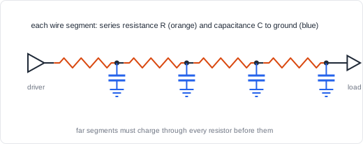
A lumped model, with all the resistance in front of all the capacitance, reaches 50% of its final voltage after about 0.69 × R × C. A distributed line is faster than that - about 0.38 × R × C - because the capacitance near the driver charges through only a small part of the resistance. Either way, delay is proportional to the product R × C.
Why wire delay grows with length squared

  R  proportional to  length
  C  proportional to  length
  delay  proportional to  R x C  proportional to  length x length

  length x2   ->  delay x4
  length x3   ->  delay x9
  length /2   ->  delay /4
Quick Check
Q: An unbuffered 1 mm wire has a delay of 25 ps. Estimate the delay of an unbuffered 3 mm wire on the same layer.
Show Answer
Delay grows with length squared: 32 = 9, so about 9 × 25 = 225 ps.
Why Wires Did Not Scale Like Transistors
When a process shrinks, transistors get faster. Wires shrink too, but a narrower, thinner wire has a smaller cross-section and therefore more resistance per millimetre. Local wires get shorter as the logic gets denser, so they keep up. Global wires, which still have to cross the whole die, do not get shorter, and their delay relative to a gate delay grows with every process generation.
Where Does Wire Delay Dominate?
In a large SoC, a bus from a processor cluster to a memory controller on the far side of the die can be several millimetres long. At gigahertz clock rates, such a wire cannot be crossed in one cycle even with ideal buffering, so architects plan for multi-cycle transfers from the start, with register stages along the route. On-chip networks that connect many IP blocks are designed around this limit.
Repeaters: Making Delay Linear
Because delay grows with length squared, splitting a long wire into shorter segments helps dramatically. Inserting a buffer (a repeater) between segments restarts the RC charging: each segment only has to charge its own capacitance through its own resistance.
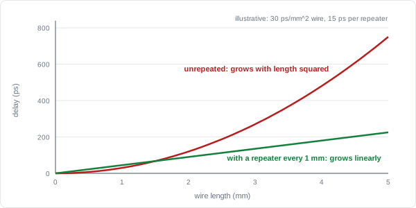
Repeater arithmetic (illustrative: 30 ps per mm^2 of wire, 15 ps per repeater)

  4 mm unbuffered   : 30 x 4^2                  = 480 ps
  4 x 1 mm segments : 4 x (30 x 1^2 + 15)       = 180 ps
  2 x 2 mm segments : 2 x (30 x 2^2 + 15)       = 270 ps

  With the segment length fixed, total delay grows LINEARLY with wire length.
  Too many repeaters add buffer delay, area and power; there is an optimum spacing.
Upsizing the driver alone does not fix a long wire. A stronger driver reduces the driver's own resistance, but the wire's resistance is still in series with every picofarad of wire capacitance. Only splitting the wire attacks the quadratic term.
Repeaters in Practice
The best repeater spacing is a compromise, and real numbers show how it works. For a wire on a middle metal layer in a 65 nm process (200 Ω/mm and 0.2 pF/mm, with a 15 ps FO4 inverter delay), a text such as CMOS VLSI Design works out an optimally repeated wire at about 41 ps per mm. That needs a repeater about every 0.45 mm, each driven by a large inverter (about 180 times the minimum size).
| Design goal | Spacing | Delay per mm | Energy per bit per mm |
|---|---|---|---|
| Minimum delay | 0.45 mm | 41 ps | 0.4 pJ |
| Minimum energy x delay | 0.8 mm | 47 ps | 0.26 pJ |
Minimum delay is expensive: the repeaters add about 87% to the switching energy of an unrepeated wire. Allowing the delay to grow by 14% lets the repeaters be spaced 1.7 times farther apart and cuts the energy a lot. Because delay is a weak function of the spacing, designers also place repeaters wherever the floorplan has room.
Practical repeater rules

  inverters as repeaters : fastest, but a wire needs an EVEN number of them
                           (or the receiver must accept an inverted signal)
  buffers (inverter pair): no polarity problem, about 8% slower per mm
  one direction only     : a repeater drives the wire one way, so bidirectional
                           and tri-state buses cannot use simple repeaters
How the Design Flow Handles Wires
The logic design never mentions wires, and logic synthesis only estimates their effect, because it does not yet know where cells will be placed. Physical implementation does the real work:
How the implementation flow handles wires

  1. Synthesis     : estimates wire load from fanout or rough placement
  2. Placement     : cells get real positions -> wire lengths become known
  3. Optimization  : insert repeaters on long nets, upsize drivers,
                     assign long nets to upper (lower-resistance) metal layers
  4. Routing       : real wire shapes are drawn
  5. Extraction    : R and C of every wire are computed from the layout
  6. Timing sign-off with the extracted parasitics
What the designer can do is make sure no single-cycle path has to cross the whole chip. If a signal must travel far, add register stages so each cycle only covers part of the distance. A chain of register slices adds one cycle of latency per stage but no logic:
Register slices along a long route (3 stages)

  source --> [FF] ---- wire ----> [FF] ---- wire ----> [FF] --> destination
              hop 1                hop 2                hop 3

  each clock cycle the data advances one hop
  each hop is 1/3 of the length, so its wire delay is only about 1/9 of the
                   whole route's (delay grows with the square of length)
  cost           = 3 cycles of latency and W x 3 flip-flops for a W-bit bus
The benefit comes only if place-and-route spreads the stages along the route, so large designs often guide the placement of such slices. The cost is latency, which the surrounding protocol must tolerate.
Where Are Register Slices Used?
On-chip interconnect fabrics insert register slices on long links between blocks, trading a cycle or two of latency for a higher clock rate. Clock distribution uses thick upper metal and carefully spaced repeaters to keep edges sharp across the whole die.
Common Mistakes
Mistake #1: Assuming wire delay grows linearly with length
For an unbuffered wire, doubling the length multiplies the delay by about four, not two. Linear scaling only appears once repeaters are inserted at a roughly fixed spacing.
Mistake #2: Trusting timing from synthesis alone
Synthesis uses estimated wire loads. After placement, long nets can be much slower than predicted. Timing is not closed until it has been checked with parasitics extracted from the real layout.
Mistake #3: Fixing a long wire by upsizing only the driver
A bigger driver helps with the load but not with the wire's own distributed resistance. For long wires, repeaters and upper metal layers are the effective fixes.
Mistake #4: Planning single-cycle paths across the whole die
At high clock rates, crossing a large die can take more than one cycle even with optimal repeaters. If the architecture assumes a one-cycle transfer, no amount of physical optimization will close timing. Plan register stages into the architecture.
Practice Exercise
Challenge: Buffer a Long Route
On a certain metal layer, an unbuffered wire has a delay of 30 ps per mm2 of length squared, and each repeater adds 15 ps.
- What is the delay of an unbuffered 6 mm wire?
- What is the delay with repeaters every 1 mm, and every 1.5 mm?
- The design runs at 1 GHz, and 400 ps of each cycle is already used by logic at both ends. Can this route be a single-cycle path?
Hint
Each segment of length s costs 30 × s2 + 15 ps. Count the segments.
Solution
1. Unbuffered: 30 x 6^2 = 1080 ps

2. Every 1 mm  : 6 segments x (30 x 1   + 15) = 6 x 45    = 270 ps
   Every 1.5 mm: 4 segments x (30 x 2.25 + 15) = 4 x 82.5  = 330 ps

3. Cycle = 1000 ps; 400 ps used by logic leaves 600 ps.
   Buffered wire (270 ps) fits; unbuffered (1080 ps) never could.
   With less margin, a register slice in the middle would split the route.
Summary
In this tutorial, you learned:
- On-chip wires have resistance and capacitance, both proportional to length
- Wire delay is proportional to R x C, so an unbuffered wire's delay grows with length squared
- A distributed RC line reaches 50% in about 0.38 RC, about half the lumped-model estimate
- Global wires get relatively slower with each process generation, while local wires keep up
- Repeaters split long wires into segments and make delay grow linearly with length
- Place-and-route inserts repeaters and picks metal layers; the design should add register stages for long cross-chip paths
