
Every gate takes a finite time to respond: its output changes some time after its input changes. That time is its propagation delay. Delays add up along a chain of gates, and the longest chain between two flip-flops - the critical path - decides the shortest clock period, and therefore the highest frequency, a design can run at. Static timing analysis tools find and report critical paths automatically, and much of digital design for speed is about keeping them short.
13 min read | Intermediate Level
What You'll Learn
- What propagation delay and contamination delay mean for a gate and for a path
- How the critical path sets the maximum clock frequency
- How static timing analysis finds critical paths without simulation vectors
- How a gate's delay depends on the load it drives, and what the fanout-of-4 inverter delay is
- Design techniques that shorten the critical path: balanced trees, less priority logic and pipelining
Gate Delay: Two Numbers
A gate's delay is measured from the moment its input crosses 50% of the supply to the moment its output crosses 50%. Two values matter:
| Delay | Meaning | Used for |
|---|---|---|
| Propagation delay (tpd) | The longest time before the output settles to its final value | Setup checks: will data arrive in time? |
| Contamination delay (tcd) | The shortest time before the output starts to change | Hold checks: will new data arrive too early? |
A gate's delay is not one fixed number. It depends on the load it drives, how sharp its input edge is, whether the output is rising or falling, and the process, voltage, and temperature corner. Timing libraries store delay tables for every cell and every corner so tools can compute each case.
Gate Delay Depends on the Load
A gate is slow when it drives a lot of capacitance. Delay is usually written in normalized form as d = g × h + p, where h is the fanout (load capacitance divided by input capacitance), g is the gate's logical effort (how much weaker the gate drives than an inverter with the same input capacitance), and p is its parasitic delay (the delay with no load). The unit is τ, the delay of an ideal inverter driving one copy of itself.
The reference point is the fanout-of-4 (FO4) inverter: an inverter driving four identical inverters. With g = 1, h = 4 and p = 1 its delay is 5τ. In a 65 nm process, where τ is about 3 ps, that is about 15 ps. Designers quote path delays in FO4 units because the number stays nearly the same from one process to the next.
| Gate (FO4 load) | Logical effort g | Parasitic delay p | Delay d = 4g + p | Delay at τ = 3 ps |
|---|---|---|---|---|
| Inverter | 1 | 1 | 5.0 τ | 15 ps |
| 2-input NAND | 4/3 | 2 | 7.3 τ | 22 ps |
| 2-input NOR | 5/3 | 2 | 8.7 τ | 26 ps |
A NAND gate is faster than a NOR gate with the same inputs because its series transistors are NMOS, which are stronger than PMOS (see CMOS NAND Gate and CMOS NOR Gate). As a rule of thumb, the FO4 delay in picoseconds is one third to one half of the drawn channel length in nanometres. Sizing gates to balance this load is covered in Gate Sizing & Drive Strength.
Delay is also sensitive to process, supply voltage and temperature. FO4 delays are normally quoted for typical process and the worst environment: low supply voltage and high temperature.
Path Delay and the Critical Path
A timing path starts at a launching flip-flop, passes through combinational gates and wires, and ends at a capturing flip-flop. Its delay is the sum of all gate delays and wire delays along the way. Between two flip-flops there are usually many paths, and the slowest one sets the limit:
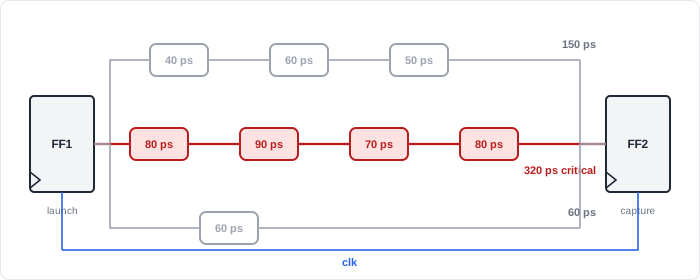
Path delay in proportions

  path delay = sum of gate delays + sum of wire delays along the path

  more logic levels         -> longer path
  larger fanout on a net    -> slower driver on that stage
  longer wires              -> more RC delay
  the path with the MOST DELAY is critical, not necessarily the one with the most gates
From Critical Path to Clock Frequency
Data launched by one clock edge must reach the capturing flip-flop, and be stable for its setup time, before the next edge. So the clock period has to cover three things for the critical path:
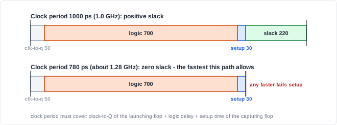
Minimum clock period (ignoring clock skew)

  clock period  >=  clock-to-Q (launch flop)  +  critical path logic delay  +  setup time (capture flop)

  Example:   50 ps + 700 ps + 30 ps = 780 ps
             maximum frequency = 1 / 780 ps = about 1.28 GHz
             at 1.0 GHz (1000 ps period): slack = 1000 - 780 = 220 ps
Positive slack means the path meets timing with margin; negative slack means it fails. Real analysis also accounts for clock skew, clock uncertainty, and on-chip variation, which take a bite out of the budget.
Hold checks are the opposite concern: the shortest path must not deliver new data so quickly that it corrupts the value the capturing flip-flop is still holding. Hold is checked with contamination delays and does not depend on the clock period, so slowing the clock never fixes a hold violation.
Quick Check
Q: A design has clock-to-Q = 40 ps and setup = 20 ps. Its critical path is 540 ps. Can it run at 2 GHz?
Show Answer
No. It needs 40 + 540 + 20 = 600 ps per cycle, which allows at most about 1.67 GHz. A 2 GHz clock has a 500 ps period, giving a slack of -100 ps.
How Tools Find the Critical Path: Static Timing Analysis
Checking timing by simulation would require input patterns that exercise the slowest path, which is impractical for large designs. Static timing analysis (STA) instead computes the worst-case arrival time at every point in the circuit directly from the cell and wire delays, without any test vectors. It checks every path in four groups: input to register, register to register, register to output, and input to output.
Simplified STA path report (illustrative format)

  Startpoint : u_ctrl/state_reg[2]   (rising edge of clk)
  Endpoint   : u_alu/result_reg[7]   (rising edge of clk)

  Point                                    Incr (ps)   Arrival (ps)
  clock clk rise edge                          0             0
  u_ctrl/state_reg[2]/Q  (clock-to-Q)         50            50
  u_dec/U14/Y            (NAND2)              38            88
  u_dec/U22/Y            (AOI21)              61           149
  u_alu/add_0/.../CO     (adder carry chain) 520           669
  u_alu/U87/Y            (MUX2)               81           750
  u_alu/result_reg[7]/D                        0           750
  data arrival time                                        750

  clock clk rise edge                       1000          1000
  setup time                                 -30           970
  data required time                                       970
  slack (MET)                                              220
Reading a report like this top to bottom shows exactly where the time goes. Here the adder's carry chain is by far the largest contributor, so that is where to look for improvement.
Where Does the Critical Path Matter?
A processor's rated frequency is set by its slowest register-to-register paths at the worst-case corner. During implementation, timing closure is an iterative loop: run STA, find the paths with negative slack, fix them by resizing gates, buffering, restructuring logic, or changing the logic, then run STA again. Large SoCs track thousands of failing paths early in this process and drive the count to zero before tape-out.
Shortening the Critical Path
Implementation tools can resize and buffer gates, but the logic depth chosen by the designer sets a floor they cannot go below. Three design techniques shorten paths directly.
1. Balance the logic: trees instead of chains
Adding four operands A, B, C, D

  Chain : ((A + B) + C) + D     3 adders in series   -> 3 adder delays
  Tree  : (A + B) + (C + D)     2 levels             -> 2 adder delays
          (the first two adders work in parallel)

  Same three adders, same result: only the arrangement changed
Tools often rebalance multi-operand additions on their own, and may use carry-save structures, but drawing the tree makes the intent explicit and does not depend on tool settings.
2. Avoid unnecessary priority
Priority logic for four requests R0 (highest) to R3 (lowest)

  Check R0 first; if not set check R1; then R2; otherwise R3
  -> a chain of multiplexers, and R3's path goes through every level

If the requests are guaranteed one-hot (never two at once), no ranking is needed:

  G1 = R2 + R3
  G0 = R1 + R3
  -> one OR gate per output bit, constant depth
A chain of "if this, else if that" conditions is a priority encoder: the conditions are checked in order, and the last condition's path goes through every level before it (see Encoder). When the conditions are mutually exclusive, a parallel structure such as the flat OR encoder above gives the same result with less depth. When priority is genuinely needed, keep the chain short and put the latest-arriving signal at the top.
3. Pipeline: cut the path with registers
Two-stage pipelined sum of A, B, C, D

  stage 1 (registered):  S_AB = A + B       S_CD = C + D      (in parallel)
  stage 2 (registered):  Y    = S_AB + S_CD

  each stage holds at most one adder between two registers
Pipelining adds a register in the middle of a long path, so each stage only has to fit part of the logic into one clock cycle. The cost is latency: the result appears one cycle later, and the surrounding logic must account for that. This is how high-frequency processors and DSP datapaths reach their clock rates.
| Technique | Critical path | Latency | Area |
|---|---|---|---|
| Chain of 3 adders | 3 adders | Same cycle | 3 adders |
| Balanced tree | 2 adders | Same cycle | 3 adders |
| Tree + 1 pipeline stage | 1 adder | +1 cycle | 3 adders + registers |
Where Is Pipelining Used?
Processor cores split instruction execution into many pipeline stages so that each stage's logic fits in a short clock period. Video, image, and audio processing datapaths are deeply pipelined, often with a register after every multiplier and adder, because throughput matters far more than the latency of a single sample.
Common Mistakes
Mistake #1: Assuming the path with the most gates is the critical one
A short path through a heavily loaded net, a long wire, or a slow complex gate can be slower than a longer chain of fast, lightly loaded gates. Only timing analysis with real loads and wire delays identifies the critical path reliably.
Mistake #2: Treating a passing functional simulation as proof of timing
A functional simulation uses ideal gates with no delays, so it cannot show setup or hold failures. Functional correctness and timing correctness are checked separately: simulation for function, static timing analysis for timing.
Mistake #3: Forgetting clock-to-Q and setup in the budget
The logic does not get the whole clock period. Clock-to-Q of the launching flip-flop, setup of the capturing flip-flop, skew, and uncertainty all come out of it first. Estimating frequency from logic delay alone is optimistic.
Mistake #4: Trying to fix hold violations by slowing the clock
Hold depends on the shortest path and on clock skew, not on the clock period. A hold violation fails at every frequency. It is fixed by adding delay to the short path, usually by inserting buffers.
Practice Exercise
Challenge: Find fmax and Pipeline Wisely
A block has clock-to-Q = 40 ps and setup = 25 ps. Its three register-to-register paths have logic delays of 610 ps, 480 ps, and 350 ps.
- What is the maximum clock frequency?
- You pipeline the 610 ps path by adding a register that splits it into 320 ps and 290 ps. What is the new maximum frequency?
- Why did the frequency not improve as much as splitting the 610 ps path might suggest?
Hint
The clock period must cover the worst path after the change. Check every path, not just the one you split.
Solution
1. Critical path = 610 ps
   Minimum period = 40 + 610 + 25 = 675 ps  -> fmax = ~1.48 GHz

2. Paths are now 320, 290, 480 and 350 ps.
   New critical path = 480 ps
   Minimum period = 40 + 480 + 25 = 545 ps  -> fmax = ~1.83 GHz

3. Once the 610 ps path was split, the 480 ps path became critical.
   Performance is always limited by the worst remaining path, so
   speeding up one path helps only until the next path takes over.
Summary
In this tutorial, you learned:
- Propagation delay is the longest time for a gate's output to settle; contamination delay is the shortest time before it starts to change
- A path's delay is the sum of its gate and wire delays; the slowest register-to-register path is the critical path
- The clock period must cover clock-to-Q, the critical path's logic delay, and setup time; the remainder is slack
- Static timing analysis checks every path without simulation vectors and reports where the time goes
- A gate's delay is d = g × h + p; an FO4 inverter has a delay of 5τ, about 15 ps in a 65 nm process
- Balanced trees, removing unnecessary priority, and pipelining shorten critical paths
- A chain of priority conditions is a priority encoder whose depth grows with every condition
- Hold violations depend on the shortest paths and cannot be fixed by slowing the clock