
An SoC uses several kinds of memory at once, because no single technology wins on every measure. Registers are fastest, SRAM is fast and sits on the chip, ROM holds code that never changes, DRAM gives large capacity cheaply, and flash keeps data when the power is off. Choosing which data lives in which memory is one of the basic decisions of system design, and memory often takes more of the chip than all the logic together. This article explains each kind of memory, how on-chip memories are organized and built, shows what they cost in area, and shows how a system places its code and data.
13 min read | Beginner
What You'll Learn
- Describe registers, SRAM, ROM, DRAM and flash and what each is used for
- Explain volatile and non-volatile memory and which memories need refresh
- Describe how an on-chip memory is organized in words, ports and macros
- Estimate the area of an on-chip memory and assign code and data to memories
Five Kinds of Memory
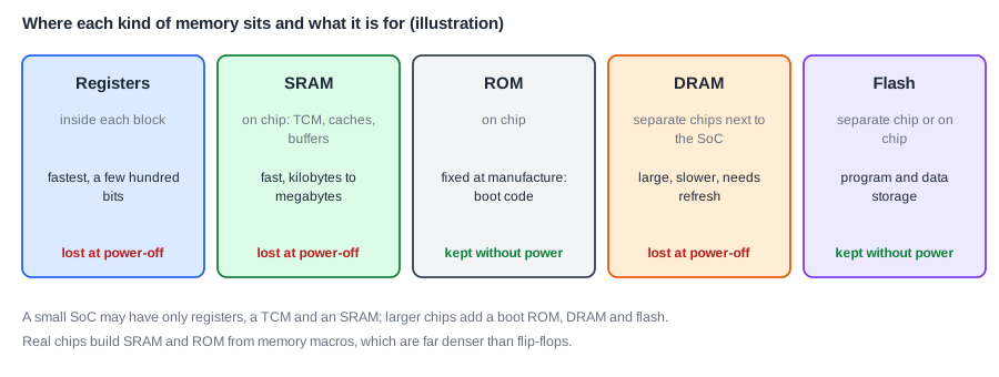
Two properties separate memory technologies at first sight. Volatile memory loses its contents when the power is switched off; non-volatile memory keeps them. And some memories are on the same die as the processor, while others are separate chips connected through package pins and board wires, which makes them slower to reach.
Registers
Registers are built from flip-flops inside each block: the processor's register file, a peripheral's control registers, the state of a bus interface. They are read and written within a clock cycle and are the fastest storage there is, but each bit is a complete flip-flop, the most expensive storage per bit. They are volatile.
SRAM
SRAM, static random-access memory, is the main on-chip memory: caches, tightly coupled memories (TCMs), buffers and scratchpads. Each bit is a cell of six transistors, two cross-coupled inverters that hold the value plus two access transistors, as The 6T SRAM Cell shows. "Static" means it holds its value as long as power is on, without refresh. "Random access" means any word can be read in the same time, whatever its address. SRAM is fast and built in the same process as the logic, but each cell is large compared with DRAM. It is volatile.
ROM
ROM, read-only memory, holds content fixed when the chip is manufactured, usually the boot code that runs first after reset and loads the rest of the software. It cannot be changed, so a bug in it is permanent: boot ROMs are kept small and verified with great care. It is non-volatile.
DRAM
DRAM, dynamic RAM, stores each bit as charge on a tiny capacitor with a single transistor. The cells are far smaller than SRAM cells, so DRAM gives gigabytes cheaply. But the charge leaks away, so every row must be read and rewritten, refreshed, every few tens of milliseconds, which is what "dynamic" means; DRAM Cell and Refresh explains it. DRAM is made in a special process, so it sits in separate chips next to the SoC, reached through a memory controller and a PHY, with a latency of tens of nanoseconds or more. It is volatile.
Flash
Flash stores charge on an insulated gate that keeps it for years without power. It holds programs, settings and files: the firmware of a microcontroller, the storage of a phone. It reads reasonably fast but writes slowly, erases in large blocks, and wears out after a limited number of erase cycles. It is non-volatile. Microcontrollers often have flash on the die; larger SoCs use separate flash chips.
| Memory | Where | Keeps data without power | Typical use |
|---|---|---|---|
| registers | inside each block | no | working values, device control |
| SRAM | on chip | no | caches, TCM, buffers |
| ROM | on chip | yes (fixed) | boot code |
| DRAM | separate chips | no, and needs refresh | main memory, gigabytes |
| flash | on chip or separate | yes | firmware, files |
Quick Check
Q: A product must keep its firmware through a power cut and still let the vendor update it. Which memory holds the firmware, and what is ROM used for in such a product?
Show Answer
Flash: it keeps data without power and can be rewritten. ROM cannot be updated, so it holds only the small boot code that runs after reset, checks the firmware in flash and starts it.
How an On-Chip Memory Is Organized
An on-chip memory is an array of words, each as wide as the data it delivers in one access. A 64 KB TCM might hold 16,384 words of 32 bits. Its size is described as depth x width: 16,384 x 32. A 14-bit word address selects one of the 16,384 rows; for a byte address, that is address bits 15 to 2, as Memory, Addresses and Endianness explains.
A memory's ports say how many accesses it can do per cycle. A single-port memory does one read or one write per cycle. A TCM usually needs two: the processor fetches an instruction and accesses data in the same cycle. It therefore has one port that can read or write, for data, and one read-only port, for instructions, an organization called 1rw1r. Every extra port costs area, so designers add ports only where the system needs them.
Large memories are not drawn gate by gate. They are macros: ready-made blocks containing the cell array, the address decoders, the sense amplifiers that read the small signals of the cells, and the write drivers, produced by a memory compiler for the requested depth, width and ports. The chip design places each macro as one rectangle, and synthesis treats it as a black box.
What Memory Costs in Area
A designer can also write a memory as an array in RTL and let synthesis build it from flip-flops. For small structures, such as a register file or a FIFO of a few entries, that is the normal choice. For large ones it is not. Take an older 130 nm process as an example. One flip-flop alone takes about 27 µm². An SRAM macro, a ready-made memory block, takes about 23 µm² per bit at 1 KB and about 17 µm² per bit at 2 KB.
Two things stand out. The macro's area per bit already includes its decoders, sense amplifiers and both ports, while the flip-flop figure covers only the storage: a flip-flop memory also needs a write enable per word and large read multiplexers to pick one word out of thousands. And the macro gets denser as it grows, by about a quarter when the size doubles, because the fixed periphery is shared by more cells. Foundry memory compilers, used for commercial chips, are typically denser still.
Now apply that to a 64 KB TCM, which is 524,288 bits. Built from flip-flops, it would be about one and a half times the size of the same memory built from macros, before counting its read multiplexers. And even built from macros, it would be about 91 times the area of a small five-stage processor core that uses it.
The core is not the expensive part. This is typical: in most SoCs, memories take a large share of the die, often more than all the logic together. That is why every kilobyte of cache or buffer in a spec is a cost decision, paid in area, leakage power and manufacturing test time.
Where Does This Matter?
Architects size caches and buffers knowing their area, and memory compilers offer only certain shapes and port counts, so a 48 KB buffer may in practice become three 16 KB macros, or a 64 KB one. Memories also need their own test logic: built-in self-test (BIST) circuits that write and read patterns into every cell after manufacture, because a single bad cell in millions would otherwise go unnoticed.
Caches and TCMs: Who Decides What Is Close
A system can put fast memory next to the processor in two ways. A tightly coupled memory (TCM) is an ordinary memory at a fixed address range; software decides what goes there, through the linker, which places code, stack and data at chosen addresses. Its timing is fully predictable: every access takes the same cycle count. A cache has no address range of its own. It sits in front of a larger, slower memory and keeps copies of the data that was used recently, chosen automatically by hardware. Software does not need to know it is there, but whether an access is fast depends on what ran before, so timing varies.
Both are common, often in the same chip. Real-time controllers, for example in cars and disk drives, use TCMs for code whose timing must be guaranteed. Application processors rely on caches, because their programs are too large and varied to place by hand. The Memory Hierarchy and Locality explains why caches work as well as they do.
When Bits Go Wrong: Parity and ECC
A memory bit can flip by itself. An alpha particle from the package material or a neutron from cosmic rays can deposit enough charge in an SRAM or DRAM cell to change its value. Such a soft error does not damage the chip; the next write repairs it, but until then the data is wrong. The more bits a chip holds, the more often this happens, so large memories, and memories in cars, servers and aircraft, are protected.
The simplest protection is a parity bit per word, chosen so that the number of 1s is always even. A single flipped bit makes it odd, so the error is detected, but parity cannot say which bit flipped. An error-correcting code (ECC) adds more check bits. The common SECDED code (single error correction, double error detection) protects a 32-bit word with 7 extra bits, 39 bits in all: it corrects any single flipped bit on the fly and detects any two. The price is about 22 percent more storage, plus encoding and checking logic in the memory path, which can add a cycle of latency. Whether a memory needs parity, ECC or nothing is a system decision recorded in the spec.
Placing Code and Data
A system decides where each kind of content lives by its size, how often it is accessed, whether other managers must reach it, and whether it must survive power-off:
| Content | Typical home | In a small SoC |
|---|---|---|
| boot code | ROM | loaded into the TCM in simulation |
| firmware and applications | flash, copied into RAM or run from it | loaded into the TCM |
| stack and frequently used data | TCM or cache | TCM, 1 cycle per access |
| large buffers, data shared with other managers such as DMA | on-chip SRAM or DRAM | system SRAM, 4 cycles per access |
The placement shows up directly in run time. In one test, the same copy program ran 22 percent slower with its destination buffer in the system SRAM than in the TCM, only because of where the buffer lives. Latency and Bandwidth works through that difference access by access.
A small CPU subsystem also makes a placement decision in hardware on every load: if the address is in the TCM's range, the data comes from the TCM; otherwise the load goes out on the bus and the data comes back from there. That small multiplexer is what makes the TCM and the rest of the memory map look like one address space to the program.
Quick Check
Q: Why would a small SoC keep the stack in the TCM rather than in the system SRAM?
Show Answer
The stack is accessed constantly, on every function call and whenever the compiler runs out of registers. In the TCM each access takes 1 cycle; in the system SRAM it would take 4 and go over the shared bus.
Common Mistakes
Mistake #1: Synthesizing large memories from flip-flops
A large array written in RTL becomes hundreds of thousands of flip-flops and multiplexers if synthesis has no macro to map it to: a huge, slow, power-hungry block. Large memories must be memory macros, instantiated or mapped deliberately.
Mistake #2: Assuming RAM keeps its contents
SRAM and DRAM lose everything at power-off, and DRAM needs refresh even while powered. Anything that must survive goes to flash or another non-volatile memory.
Mistake #3: Sizing memories from the spec alone
A memory compiler offers specific depths, widths and port counts. Check what the compiler can produce, and its area, before the size goes into the architecture spec.
Practice Exercise
Challenge: The Cost of the System SRAM
A system SRAM holds 16 KB as 4,096 words of 32 bits, with a single port. (a) How many bits is that, and how much area would the storage take at 27 µm² per flip-flop? (b) How much area would it take at 17 µm² per bit in macros (even though those have two ports)? (c) Compare both with a processor core of 0.1 mm², which is 100,000 µm². (d) Which port organization does the system SRAM need, and why is it different from the TCM's?
Hint
16 KB is 16 x 1,024 x 8 bits.
Solution
(a) 131,072 bits; 131,072 x 27 µm² = 3,538,944 µm², about 3.5 mm², for the flip-flops alone. (b) 131,072 x 17 µm² = 2,228,224 µm², about 2.2 mm². (c) About 35 and 22 times the core. (d) A single port, because only one access arrives at a time, over the bus from one manager. The TCM needs two because the core fetches an instruction and accesses data in the same cycle.
Summary
- Registers, SRAM, ROM, DRAM and flash each win on a different measure; systems use all of them.
- ROM and flash keep data without power; SRAM and DRAM do not, and DRAM also needs refresh.
- On-chip memories are depth x width arrays with one or more ports, built as macros by a memory compiler.
- SRAM macros are denser than flip-flops, yet a 64 KB TCM would still be about 91 times the area of a small core.
- Code and data are placed by size, speed, sharing and persistence: the stack in the TCM, shared buffers in system SRAM.
