
Chiplets are separate dies, made apart and joined inside one package so that together they work as one system. For decades, putting more onto a single die was the way to make a system cheaper and faster. Very large dies are now expensive to make, and some parts of a system don't benefit from the newest manufacturing process, so many products split the system across several dies instead. This article explains why a die's size matters for cost, what a package does, the ways dies are joined in a package, what crosses between them, and how an architect decides what goes on which die.
12 min read | Intermediate
What You'll Learn
- Explain how die size affects yield and cost
- Describe what a package does and the main package types
- Compare ways of joining dies: substrate, interposer, bridge and stacking
- Decide how to partition a system across chiplets
Why Die Size Matters
Chips are made many at a time on a round silicon wafer, and every wafer has some defects scattered across it. A die that contains a defect is usually lost. If defects are spread at random, a small die is likely to miss them all, while a large die is likely to catch at least one. A common first estimate of the fraction of good dies is:
yield = e^(-area x defect density)
With an assumed defect density of 0.1 per square centimetre, a 1 cm2 die yields about e-0.1, 90 percent, but a 6 cm2 die yields only about e-0.6, 55 percent. These values are assumptions for this example. Large dies also waste more of the round wafer at its edge. The cost per good die therefore rises faster than its area. There is also a hard limit: the area a lithography machine can expose at once, about 8.6 cm2 on current machines, so no single die can be bigger than that.
Splitting the same logic into four dies of 1.5 cm2 each gives each die a yield of about e-0.15, 86 percent. Each die is tested on its own, and only good ones are put into packages. Much less silicon is thrown away. This is the first reason for chiplets.
Mixing Processes
The second reason is that not every part of a system needs the newest process. Processor cores and caches benefit greatly from smaller transistors. Analog circuits, I/O drivers that must handle higher voltages, and the physical layers of interfaces such as DDR and PCIe shrink little from one process to the next, yet cost just as much per square millimetre on the new process. Putting them on a separate die, made in an older, cheaper process, saves money and lets the same I/O die be reused across several products.
A third reason is reuse. A company can make one compute die and combine one, two or four of them with an I/O die to build a range of products, from a desktop processor to a large server part, without designing a new die for each. Each die is verified and taped out once, and a later product can update one die while keeping the others.
Quick Check
Q: Using yield = e-area x defect density with 0.2 defects per cm2, what is the yield of a 4 cm2 die and of a 1 cm2 die?
Show Answer
4 cm2: e-0.8, about 45 percent. 1 cm2: e-0.2, about 82 percent. Four small dies waste far less silicon than one large one, since each bad small die loses only a quarter of the area.
What a Package Does
A die can't be soldered to a board directly. The package holds it, protects it, carries signals and power between the die's tiny pads and the board's much larger connections, and carries heat away. Its wiring is called the substrate: a small board with fine layers of copper. Dies connect to it either with fine wires from pads at the die's edge, called wire bonding, or face down through small solder balls across the whole die, called flip-chip. Flip-chip allows thousands of connections and short power paths, so nearly all large chips use it. The package then connects to the board through a grid of larger balls underneath.
Power delivery is one of the package's hardest jobs. A large processor can draw hundreds of amperes at under 1 V, so the supply must reach the die through many parallel paths with little resistance and inductance, and the package holds capacitors close to the die to supply sudden changes in current. Heat goes the other way, through the back of the die, a lid and a heat sink. The package design is planned with the chip, not after it. The positions of the die's power and signal bumps must match the package's routing, so the two teams agree on a bump map early, and a change on either side affects the other.
Joining Dies
Several dies in one package need connections between them. There are four main ways, with very different density and cost:
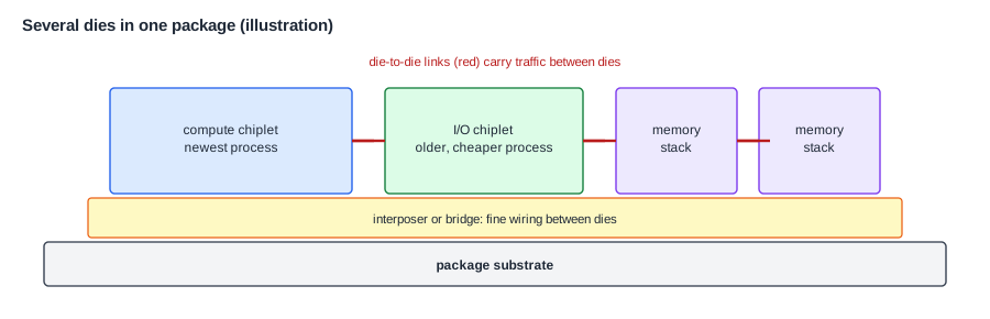
- Through the organic substrate: dies sit side by side on the package substrate, and its copper layers connect them. Cheap, but the wires are relatively coarse, so the number of connections per millimetre of die edge is limited.
- Silicon interposer: a large, simple piece of silicon with very fine wiring, on which the dies sit side by side. It allows many times more connections and is used, for example, to connect processors to stacks of high-bandwidth memory. It adds cost, and its own size is limited.
- Embedded bridges: small pieces of silicon set into the substrate only under the edges of neighbouring dies, giving fine wiring where it is needed without a full interposer.
- 3D stacking: one die on top of another, joined through vertical connections, through-silicon vias, or by bonding the two surfaces directly. The shortest links and the most connections, but heat from the lower die must pass through the upper one, and both must be designed together.
Memory stacks are an example of 3D stacking already common in products: high-bandwidth memory stacks several DRAM dies on a base die, with thousands of connections, and sits beside the processor on an interposer.
What Crosses Between Dies
Inside a die, wires are cheap and the interconnect can be as wide as needed. Between dies, each connection needs a bump, a driver and a receiver, so connections are limited, and each bit costs energy to send. Die-to-die links therefore run each wire fast, many gigabits per second, and the logic on both sides packs bus transactions into packets for the link, much like a network-on-chip, as Buses, Crossbars and Networks-on-Chip describes. Open standards for these links, such as UCIe, let dies from different companies work together.
The link adds latency, a few nanoseconds each way, and uses more energy per bit than an on-die wire, though far less than going off the package to another chip. An architect must cut the system where the traffic is lowest. Splitting a core from its level-one cache would be a disaster; splitting the cores from the I/O controllers, which see much less traffic, works well. The memory controller is often a hard choice: next to the memory interface on the I/O die, all the compute dies' memory traffic crosses the link, so the link must be sized for the full memory bandwidth from Memory Bandwidth Budgets.
Where Is This Used?
Many current desktop and server processors are built from several compute dies and an I/O die in one package; server parts with many cores use more compute dies. Graphics processors and accelerators for machine learning sit next to stacks of high-bandwidth memory on interposers. Some processors stack a large cache die directly on top of the compute die to triple its cache. Phones mostly still use one large SoC die, with memory stacked on top in the same package.
Partitioning the System
Deciding what goes on which die is an architecture decision, made early, with numbers. The architect lists the blocks, estimates each one's area on each possible process, and maps the traffic between them. Then candidate partitions are compared on:
- Cost: the yield and cost of each die, the package and the assembly, including dies lost in assembly.
- Performance: the bandwidth and latency of each cut, and whether the links can carry the traffic.
- Power: the energy spent on die-to-die traffic, which can be a noticeable share.
- Reuse: which dies can serve more than one product.
- Risk and schedule: each die needs its own tapeout, and the dies must work together the first time.
Chiplets also change testing. A faulty die found after it has been assembled into a package wastes the good dies in the same package, so each die must be tested thoroughly before assembly; dies that pass are called known good dies. The die-to-die links themselves need test and repair, often with spare lanes. Design for test, covered in Design for Test at SoC Level, must reach across dies.
Quick Check
Q: A package holds four dies, each with a 2 percent chance of being faulty if it is not tested before assembly. What fraction of packages would contain at least one bad die?
Show Answer
The chance that all four are good is 0.984, about 0.92, so about 8 percent of packages would have a bad die and waste three good ones with it. That is why each die is tested before assembly.
Designing Across Dies
Several dies must also be designed as one system. Their clocks are usually separate, so the links cross clock domains. Power-up and reset must be coordinated, so that no die drives a link before the other is ready. The address map spans dies, and coherence, if the cores on different dies share memory, runs over the links, which adds latency to snoops, as Multicore Integration and Coherent Interconnects explains. Software may need to know which memory is near which core, since accesses that cross dies are slower.
Thermal and mechanical design matter more too. Dies of different thickness and material expand differently as they heat, which stresses the bumps between them. Hot compute dies next to cooler I/O dies give an uneven temperature across the package. These effects are modelled together with the package supplier long before the first part is built.
Common Mistakes
Mistake #1: Cutting where the traffic is high
A die-to-die link has far less bandwidth and more latency than on-die wires. Cut the system where the traffic between the parts is lowest.
Mistake #2: Ignoring package and assembly cost
Smaller dies yield better, but advanced packaging, assembly and dies lost in it add cost. Compare the whole cost, not only die yield.
Mistake #3: Testing dies only after assembly
One bad die can waste the good dies packaged with it. Test each die fully before assembly.
Practice Exercise
Challenge: One Die or Four?
A design needs 6 cm2 of logic. The defect density is 0.15 per cm2, and silicon costs $10 per cm2 of wafer area before yield. Option A is one 6 cm2 die. Option B is four 1.5 cm2 dies, plus $15 of extra packaging per product. Use yield = e-area x defect density and ignore edge losses. These numbers are assumptions for this exercise. Which option is cheaper per working product?
Hint
Cost per good die = (area x $10) / yield. Option B needs four good dies.
Solution
A: yield e-0.9 = 0.41, cost $60 / 0.41 = $148. B: yield e-0.225 = 0.80 per die, cost $15 / 0.80 = $18.8 per die, $75 for four, plus $15 packaging = $90. Option B is about 40 percent cheaper, provided assembly doesn't lose many packages.
Summary
- Yield falls quickly with die area, so large dies are expensive, and no die can exceed the lithography field.
- Chiplets split a system into smaller dies, and let each part use the process that suits it.
- The package carries signals, power and heat; dies join through the substrate, an interposer, bridges or 3D stacking.
- Die-to-die links have less bandwidth and more latency than on-die wires, so the system is cut where traffic is low.
- Partitioning compares cost, performance, power, reuse and risk, and each die must be tested before assembly.
