
Memory-mapped I/O is how software controls hardware. Each device presents a small set of registers at fixed addresses, and the processor reads and writes them with the same load and store instructions it uses for memory. Turning on an LED, sending a byte over a serial port or starting an accelerator all come down to stores to the right addresses. This article explains device registers, their fields and access types, follows one store from the processor to the pins of a GPIO block, walks through a real UART driver, and shows with compiled code why device accesses need special care in C.
14 min read | Beginner
What You'll Learn
- Explain how devices appear as registers in the address space
- Read a register map with offsets, bit fields, access types and reset values
- Follow a store from the core through the interconnect to a device's pins
- Write C code that accesses device registers correctly, and explain volatile
Devices Live at Addresses
A processor has only a few ways to affect the world: it computes in registers, and it loads and stores at addresses. To let it control a device, an SoC gives the device an address window, a range of the address space, and places the device's registers in it. A device register is a small piece of storage, or sometimes just a set of wires, inside the device, which the processor reaches with an ordinary load or store. Reaching devices this way is memory-mapped I/O (MMIO).
The processor cannot tell a device register from memory. It sends a store to an address, and the interconnect delivers it to whichever block owns that address in the memory map. If that block is a memory, a value is stored; if it is a device, the device does something. Some processor families also have separate I/O instructions with their own address space, but RISC-V, Arm and most other modern processors use memory-mapped I/O only.
Each register has an offset from the device's base address. In a small example SoC, the UART has its base at 0x4000_0000 and its STATUS register at offset 0x004, so STATUS is at 0x4000_0004. Offsets are usually multiples of 4, so that each register is one aligned 32-bit word.
Control, Status and Data
Most device registers fall into three kinds:
| Kind | What it does | Example |
|---|---|---|
| Control | tells the device how to behave; software writes it, usually once at start-up | UART DIV (clock cycles per bit), timer compare value |
| Status | reports the device's state; the device updates it, software reads it | UART STATUS (FIFO full, busy) |
| Data | carries the data going to or coming from the device | UART TXDATA, GPIO OUT and IN |
Here is the complete register map of the peripherals in that small SoC:
| Device (base) | Offset | Register | Access | Meaning |
|---|---|---|---|---|
| UART (0x4000_0000) | 0x000 | TXDATA | write only | queue one byte for sending |
| 0x004 | STATUS | read only | bit 0: FIFO full; bit 1: busy (a byte queued or being sent) | |
| 0x008 | DIV | read/write | clock cycles per bit, reset value 16 | |
| Timer (0x4000_1000) | 0x000, 0x004 | MTIME_LO, MTIME_HI | read only | 64-bit count of clock cycles since reset |
| 0x008, 0x00C | CMP_LO, CMP_HI | read/write | 64-bit compare value; interrupt while MTIME >= CMP | |
| GPIO (0x4000_2000) | 0x000 | OUT | read/write | drives the 32 output pins |
| 0x004 | IN | read only | the current state of the 32 input pins | |
| Sim control (0x4000_F000) | 0x000 | EXIT | write only | ends the simulation; the value is the result |
A real device's register map holds the same information for every register: offset, name, access type, the meaning of each bit, and the reset value, the value it has after the chip is reset. Hardware and software are built from it, so it is one of the most important parts of the system spec, described in The System Architecture Spec.
Bit Fields
Many registers pack several small values into one word, each in its own group of bits, a field. The UART STATUS register has two one-bit fields: bit 0 is 1 when the 8-byte transmit FIFO (first in, first out buffer) is full, and bit 1 is 1 while the UART still has bytes to send. Software isolates a field with a bitwise AND against a mask that has 1s only in the field's bits: STATUS & 1 keeps bit 0, STATUS & 2 keeps bit 1. A wider field, for example bits 7 to 4, is read with a shift and a mask: (reg >> 4) & 0xF.
Access Types and Side Effects
Device registers do not behave like memory, and the access type says how they differ. A read-only register ignores writes. A write-only register returns nothing useful when read: the UART's TXDATA always reads as 0, not as the last byte written. Some registers change by themselves, like the timer's MTIME, which counts every cycle. Some reads and writes have side effects: writing TXDATA does not just store a value, it adds a byte to the FIFO and starts sending it; in many devices, reading a receive-data register removes the byte from a FIFO, and some status bits are cleared by writing a 1 to them ("write 1 to clear"). Software must access each register exactly as the register map describes.
Quick Check
Q: A program reads 0x0000_0002 from the UART STATUS register. Can it write a new byte to TXDATA, and has the UART finished sending?
Show Answer
Bit 0 (FIFO full) is 0, so there is room and it can write a byte. Bit 1 (busy) is 1, so the UART has not finished: bytes are still queued or being sent.
One Store, From Core to Pins
A small program sets the GPIO outputs with the C statement GPIO_OUT = 0xA5;, which the compiler turns into a single store instruction:
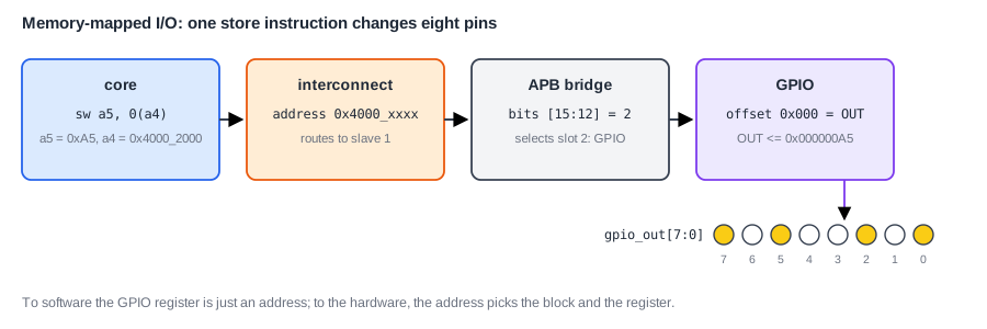
Each block on the way uses a different part of the address:
| Block | Looks at | Decision |
|---|---|---|
| CPU subsystem | the whole address 0x4000_2000 | not in the local 64 KB memory: send it out on the AXI4-Lite port |
| interconnect | the upper bits, 0x4000_xxxx | the peripheral window: pass the write to the APB bridge |
| APB bridge | bits 15 to 12, here 2 | select peripheral slot 2, the GPIO |
| GPIO | the offset, bits 11 to 0, here 0x000 | write the OUT register |
On the clock edge at the end of the transfer, OUT holds 0xA5, binary 1010 0101, and its bits drive the chip's output pins: an LED connected to bit 0 would light, one on bit 1 would stay dark. Splitting the address level by level like this is how every SoC decodes addresses, and it is why device windows are sized and aligned to powers of two.
Where Is This Used?
Every device driver, from a microcontroller's GPIO code to an operating system's network driver, is built on memory-mapped registers. In industry the register map is usually written once, in a machine-readable form such as IP-XACT or SystemRDL, and generated into RTL, C headers and documentation, so that hardware and software cannot disagree on an address or a field.
A Real Driver: Sending a Character
A small program can talk to the UART through a few lines of C. A driver is exactly this: the code that knows a device's registers and how to use them, so that the rest of the program can just call uart_putc('H'):
#define REG(a)      (*(volatile u32 *)(a))
#define UART_BASE   0x40000000u
#define UART_TXDATA REG(UART_BASE + 0x0)
#define UART_STATUS REG(UART_BASE + 0x4)

static void uart_putc(char c)
{
    while (UART_STATUS & 1)            /* wait while the FIFO is full */
        ;
    UART_TXDATA = (u32)c;
}
REG(a) turns a number into something C can read and write: it converts the address into a pointer to a 32-bit value and dereferences it. UART_STATUS & 1 then becomes a load from 0x4000_0004 and a mask of bit 0. The loop keeps reading STATUS while the FIFO is full, and once there is room, the function stores the character to TXDATA. In one test program that printed 71 characters, the loop read STATUS about 12 times per character while the UART caught up.
Why volatile Is Required
The keyword volatile in REG is essential. A C compiler assumes that memory changes only when the program writes it, and it uses that assumption to optimize: to produce fewer, faster instructions with the same result. For memory that is correct. For a device register it is wrong, because the device changes STATUS by itself. volatile tells the compiler that every access has effects it cannot see, so it must perform each read and write, in program order, exactly as written.
The difference is easy to see. Here is the same wait loop compiled by GCC 13 for RV32I with optimization level -O2, once with an ordinary pointer and once with a volatile one:
wait_plain:                            # STATUS through a plain pointer
   0:  lui   a4,0x40000
   4:  lw    a5,4(a4)                  # read STATUS once
   8:  andi  a5,a5,1
   c:  beqz  a5,14                     # not full: return
  10:  j     10                        # full: loop forever, never reread
  14:  ret

wait_volatile:                         # STATUS through a volatile pointer
  18:  lui   a4,0x40000
  1c:  addi  a4,a4,4
  20:  lw    a5,0(a4)                  # read STATUS
  24:  andi  a5,a5,1
  28:  bnez  a5,20                     # full: read it again
  2c:  ret
In the plain version the compiler reasoned that nothing inside the loop writes STATUS, so its value cannot change, so reading it once is enough. If the FIFO happens to be full at that moment, the program hangs in the jump-to-itself at 0x10. The volatile version keeps the load inside the loop and sees the bit change as the UART sends. Such bugs are hard to find, because they appear only with optimization switched on and only when the device happens to be busy.
Quick Check
Q: A program writes GPIO_OUT = 1; GPIO_OUT = 0; to send a short pulse on a pin. What could a compiler do to this code if GPIO_OUT were not volatile?
Show Answer
It could drop the first store, because its value is overwritten before anything reads it. The pin would never go high. With volatile, both stores are performed in order, and the pin pulses.
Changing One Field: Read-Modify-Write
Software often needs to change one field of a register and leave the rest alone, for example to set GPIO output bit 3 without disturbing the other 31 pins. With a plain register, the only way is a read-modify-write: read the register, change the bits, write the whole word back:
GPIO_OUT = GPIO_OUT | (1u << 3);     /* set bit 3: load, OR, store */
GPIO_OUT = GPIO_OUT & ~(1u << 3);    /* clear bit 3: load, AND, store */
Each line is three instructions: a load, an OR or AND, and a store. That is fine as long as nothing else changes the register in between. If an interrupt handler also drives GPIO pins and runs between the load and the store of the main program, the store writes back the old value of the handler's bits and silently undoes its change. Software protects such sequences by briefly disabling interrupts, and hardware designers avoid the problem with separate set and clear registers: writing a 1 to a bit of a SET register sets that output, writing a 1 to a CLR register clears it, and bits written as 0 are left alone. One store then changes exactly the intended bits, with no read at all. Many microcontroller GPIO blocks offer such registers for this reason.
When Does a Write Reach the Device?
A program assumes that its stores happen in the order it wrote them. With memory-mapped I/O this matters a great deal: a driver typically writes a data register first and then a control register that starts the device, and the device must see them in that order.
On a simple SoC this is guaranteed by construction. The CPU subsystem waits for each write's response before the core continues, so every write has reached its device before the next instruction runs. Faster systems let writes be posted: the processor moves on as soon as the interconnect has accepted the write, and writes to different devices may arrive in a different order than they were issued. Processor architectures therefore define ordering rules for device accesses, and provide instructions to enforce them where needed. RISC-V has the fence instruction, which makes all memory and device accesses before it visible before any access after it. Drivers place such barriers at exactly the points where order matters.
Common Mistakes
Mistake #1: Accessing device registers without volatile
The compiler optimizes memory accesses freely, and device accesses are not memory. Declare every device register pointer volatile, or use a header generated from the register map that already does.
Mistake #2: Reading a register to check a write
Not every register reads back what was written: write-only data registers read as something else, and some bits clear when read or written. Follow the register map, not assumptions about memory.
Mistake #3: Using the wrong access size
Many devices support only 32-bit accesses to their registers. A byte store to a device register may write the wrong byte lane or be ignored, depending on the device. Use the size the register map specifies.
Practice Exercise
Challenge: Account for Every Peripheral Access
A test program prints a 71-character report on the UART, reads the timer twice, writes the GPIO outputs once and reads the GPIO inputs once. A count of its peripheral accesses gives these rows:
  target    base            reads  writes  cycles/access
  UART      0x4000_0000      835      71     6.00
  TIMER     0x4000_1000        2       0     6.00
  GPIO      0x4000_2000        1       1     6.00
(a) Which register does each UART read and write go to? (b) On average, how many times did uart_putc read STATUS per character, and why more than once? (c) How many cycles did all UART accesses cost? (d) Which address does the GPIO read go to, and which register?
Hint
Look at uart_putc: one store per character, and a loop of STATUS reads before it. Every peripheral access costs 6 cycles.
Solution
(a) The 71 writes go to TXDATA at 0x4000_0000, one per character; the 835 reads go to STATUS at 0x4000_0004. (b) 835 / 71 = 11.8 reads per character on average: the program produces characters faster than the UART sends them (160 cycles per character at the reset setting), so once the 8-byte FIFO fills, each call loops until a byte has gone out. (c) (835 + 71) x 6 = 5,436 cycles. (d) The read goes to 0x4000_2004, the GPIO IN register, which returns the state of the input pins.
Summary
- Devices expose control, status and data registers at offsets from their base address, reached with ordinary loads and stores.
- A register map gives each register's offset, fields, access type and reset value; masks and shifts extract fields.
- A store to 0x4000_2000 is decoded level by level: CPU subsystem, interconnect, APB bridge, then the GPIO's OUT register.
- Device registers can change by themselves and accesses can have side effects, unlike memory.
- Without volatile, GCC turned a status-polling loop into a single read and an endless jump; volatile forces every access.
