
Top-level integration is the step in which all the blocks of an SoC are connected into one design: every port wired, every clock and reset delivered, every address decoded, every interrupt routed. It sounds like bookkeeping, and much of it is, but it is also where a large share of SoC bugs are made. Blocks that each work alone fail when they meet. This article explains what the top level contains, why it is generated rather than written by hand, which checks catch integration bugs, and what the most common bugs look like.
11 min read | Intermediate
What You'll Learn
- Describe what the top level of an SoC contains
- Explain why top levels are generated from a specification
- List the checks that catch integration bugs and what each finds
- Recognize the most common classes of integration bug
What the Top Level Is
The top level is the RTL module that contains everything else. It instantiates each block, such as the CPU subsystem, the interconnect, memories, peripherals and accelerators, and connects their ports with wires. It also connects the chip's pins, through I/O cells, to the blocks that use them. A small SoC's top level is a few hundred lines. A large one has thousands of instances and hundreds of thousands of connections.
Several networks run through the top level besides data:
- Clocks, from PLLs and dividers to every block, with gating for power.
- Resets, from the reset controller, in the right order, as Reset Architecture and Reset Domain Crossings explains.
- Interrupts, from every device to the interrupt controller.
- Power control, isolation and retention signals for each power domain.
- Test and debug, the scan chains, JTAG and trace.
- Configuration, the tie-offs that set a block's mode, such as its ID or its reset vector.
Any of these, wired wrong, can break the chip in ways that no block-level test would see.
Generated, Not Written
Writing thousands of connections by hand guarantees mistakes. So teams describe the system in a machine-readable form, and a tool generates the top level:
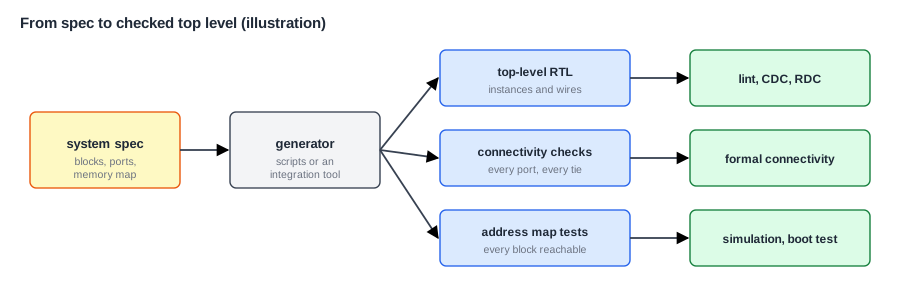
The source lists each block instance, its parameters, and how its ports connect, plus the memory map. Standards such as IP-XACT (IEEE 1685) describe blocks and their interfaces in XML, so that tools from different vendors can read them. Many companies use their own formats and scripts.
From the same source, the generator also writes the files that must agree with the top level: the interconnect's address decoder, the C header with base addresses for software, the documentation of the memory map, and tests that check every block can be reached. This is the same idea as generating register files from one description, in The System Architecture Spec. One source of truth cannot disagree with itself.
Interfaces are usually connected as bundles, rather than wire by wire: an AXI port is about 40 signals, and connecting it as one named interface removes a whole class of errors, such as swapping two signals of a channel.
Quick Check
Q: A team adds a peripheral at a new address. Which files must change, and why is a generator useful here?
Show Answer
The top-level RTL, the interconnect's address decoder, the C header for software, the memory map document and the tests. A generator changes all of them from one edit, so none of them can be forgotten or left inconsistent.
The Checks
Several kinds of check run on the integrated design. Each finds different bugs.
Lint
Lint tools read the RTL and flag suspicious code: unconnected ports, signals with several drivers, widths that don't match, such as connecting a 32-bit bus to a 16-bit port, and inputs left floating. Most are quick to fix, and some are real bugs. Lint runs on every change.
Clock and Reset Domain Checks
CDC tools find every signal that crosses from one clock domain to another, and check that it passes a proper synchronizer, as Clock Architecture and Clock Domain Crossings explains. RDC tools do the same for reset domains. These bugs don't show in ordinary simulation, which is why they need special tools.
Connectivity Checks
A connectivity check proves that each connection in the spec exists in the RTL, such as "interrupt 7 of the controller is driven by the UART's irq output". Formal tools can check thousands of such statements in minutes, against the generated top level. This catches a swapped interrupt or a block tied to the wrong reset.
Register and Address Map Tests
Simple tests run on the processor in simulation: read every register's reset value, write and read back the writable ones, and access every address region, including a few that belong to nobody, to check the error response. Memory Maps and Address Decoding shows the alias bugs these tests can find.
Because these tests are generated from the same source as the top level, every block is covered, and none is skipped by accident.
System Tests
Finally, real software runs on the integrated chip: boot code, drivers, and tests that use several blocks together, such as a DMA transfer to the UART while the timer interrupts. SoC-Level Verification Strategy covers these in detail.
Where Does This Matter?
Industry experience is consistent: a large share of the bugs found late in an SoC project are at the boundaries between blocks, in their interfaces and their connections, rather than inside the blocks. Teams therefore put a lot of automation into integration, and they run the generator and its checks every night, so that a mistake made today is caught tomorrow. A wrong pin assignment found after tape-out may be fixable on the board, but a missing interrupt usually is not.
Common Integration Bugs
A few kinds of bug appear again and again:
- Tie-offs. An input left at a default value, such as a block's ID or a mode pin, that should have been set. The block works, but in the wrong mode.
- Width mismatches. An address bus connected with the top bits missing, so that a block appears at many addresses.
- Swapped or missing interrupts. The software handler for one device runs when another device interrupts.
- Wrong clock or reset. A block clocked from the wrong source, or released from reset before its clock is running.
- Endianness or byte lanes. A block that expects a different byte order, or wrong write strobes, so that byte writes land in the wrong place.
- Different assumptions. Two blocks agree on wires, but not on meaning, such as one sending a burst type the other can't handle, or a status bit defined vaguely.
A real example from a small SoC shows the last kind. A processor core passed all its tests with memory that answered in one cycle. Inside the SoC, the bus took several cycles, and a value being forwarded inside the pipeline was lost while the core waited. The core and the bus each met their own specification, and the bug lived in the gap between them. The SoC Team and Flow describes it and two other real cases.
Quick Check
Q: A peripheral's 12-bit address input is connected to only 8 bits of the bus, with the top 4 tied to zero. What do software tests see?
Show Answer
Registers at offsets of 0x100 or more are unreachable, and accesses to them land on lower registers instead, because the top bits are always zero. Registers below 0x100 work normally, so a test that only touches the first few registers misses it.
Integration in Practice
Integration doesn't happen once, at the end. It starts early, with stub versions of blocks that have the right ports but no logic, so that the top level and its checks exist from the start. Real blocks replace the stubs as they become ready. Each new IP drop is integrated, checked and simulated before it is accepted. That early start also feeds the physical design team, who need the block list, sizes and connections to plan the floorplan.
Pins need attention as well. The pin list says which pad each signal uses, its I/O cell type, its default state at reset, and its multiplexing options. It must match the board design and the package, and it is reviewed by the board team. Pin choices often can't change late, because the package and boards are designed in parallel.
Physical Concerns at the Top Level
The top level is also where logical design meets layout. On a large chip, two blocks that are connected may sit millimeters apart, and a signal can't cross that distance in one clock cycle. So integrators add register slices, also called pipeline stages, on long interfaces, which costs a cycle of latency but meets timing. The interconnect is often split into pieces placed near the blocks they serve. The floorplan team and the integration team work together on this, because the position of each block decides which connections are long.
Each block also arrives with timing constraints for its own ports, and the top level needs constraints for every path between blocks, for clocks and for the I/O pins. Missing or wrong constraints at the top level are a common reason a chip fails timing late in the project. Power is part of it too: the top level decides which blocks share a power domain, and where isolation cells go on signals that leave a domain that can be switched off, as Power Domains and Power Management explains. All of these decisions are recorded in the same source as the connections, so that the generated files and the physical design agree, and a change to one is reflected in all the others.
Common Mistakes
Mistake #1: Editing the generated top level by hand
A hand edit is lost the next time the generator runs, and the source no longer describes the chip. Change the source, then regenerate.
Mistake #2: Skipping CDC and RDC checks
Crossing bugs pass ordinary simulation and fail in silicon, at random. Run the structural checks on every release of the top level.
Mistake #3: Testing only the first register of each block
Width and decoding bugs often affect only higher offsets. Test every register and some unused addresses in each block's range.
Practice Exercise
Challenge: Find the Integration Bugs
A review of a small SoC's top level finds these facts. (1) The SPI controller's interrupt goes to input 5 of the interrupt controller, but the spec says input 6. (2) The timer's clock comes from the 32 kHz always-on clock, but its driver assumes 100 MHz. (3) The DMA engine's write-strobe output is 4 bits, connected to an 8-bit strobe input on a 64-bit SRAM port, with the top 4 bits tied to 1. (4) The UART's reset comes from the peripheral reset, which is released before the peripheral clock starts. For each, describe the symptom software would see, and which check should have caught it.
Hint
Think about connectivity checks, register tests, CDC or RDC checks, and system tests.
Solution
(1) The SPI handler never runs, or another device's handler runs instead. A connectivity check against the spec catches it. (2) Every timeout is about 3,000 times too long. A system test measuring a delay, or a check of the clock connections against the spec, catches it. (3) Every DMA write also writes the upper 4 bytes of the 64-bit word, corrupting the neighboring data. Lint flags the width mismatch, and a DMA test with byte-level checking catches it. (4) The UART may leave reset in an unknown state, or miss its reset entirely. An RDC check and a reset-sequence review catch it, and a test on silicon may fail only sometimes.
Summary
- The top level connects every block's data, clocks, resets, interrupts, power, test and configuration signals.
- It is generated from one machine-readable source, together with the address decoder, headers, documents and tests.
- Lint, CDC, RDC, connectivity checks, register tests and system tests each catch different integration bugs.
- Common bugs are tie-offs, width mismatches, swapped interrupts, wrong clocks or resets, and different assumptions.
- Integration starts early with stubs and runs every night, so mistakes are caught when they are cheap.
