
FPGA prototyping and emulation run an SoC's design in special hardware, thousands of times faster than simulation, so that real software can run on it before the chip is made. Simulation shows every signal but is far too slow to boot an operating system on a large chip; silicon is fast but arrives months later and can't be changed. These two platforms fill the gap. This article explains how slow simulation really is for a large SoC, how emulators and FPGA prototypes work, what each is good for, and the practical problems of fitting a chip's design into them.
12 min read | Intermediate
What You'll Learn
- Explain why simulation is too slow for system software
- Describe how emulators and FPGA prototypes run a design
- Compare the platforms on speed, visibility, capacity and cost
- Identify the changes a design needs to run on an FPGA
The Speed Problem
An RTL simulator computes every signal of the design in software, cycle by cycle. For a small block, it may simulate millions of cycles per second. For a full SoC with billions of transistors, it is far slower: often a few hundred to a thousand cycles per second. Booting an operating system takes billions of cycles. At 1,000 cycles per second, a boot of two billion cycles would take two million seconds, about 23 days. Simulation is therefore limited to short tests, and software teams can't use it to develop drivers.
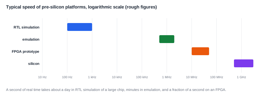
The figure shows typical speeds, which vary with the design and the platform. Each step to the right is about a thousand times faster than the one before. A second of real operation takes about a day in RTL simulation of a large chip, minutes in emulation, and a fraction of a second on an FPGA prototype running at a few tens of megahertz.
Emulation
An emulator is a large, specialized machine built to run chip designs. Some are built from arrays of custom processors that evaluate the design's logic in parallel; others from many large FPGAs. The design's RTL is compiled into the emulator's hardware, which then runs it at around a megahertz, a thousand or more times faster than simulation.
Emulators are designed for verification. They can hold very large designs, billions of gates, by combining many boards. They keep much of the visibility of simulation: signals can be captured over long windows and viewed as waveforms, and the design can be stopped and inspected. Compiling a new version of the design takes hours, not days. They can connect to the same verification components as simulation, running in a host computer, through fast links, or to real devices through speed adapters that buffer traffic between the slow emulated chip and fast real equipment, such as a network or a display.
Their drawbacks are cost and sharing. An emulator costs millions, so a company has a few and shares them between projects, and time on them is scheduled. Teams use emulation for the tasks that need it: booting operating systems, running long real workloads, measuring performance and power over realistic scenarios, and finding the bugs that only appear after billions of cycles.
Quick Check
Q: A workload takes 500 million cycles. How long does it take at 1 kHz in simulation, at 1 MHz in emulation, and at 20 MHz on an FPGA prototype?
Show Answer
Simulation: 500,000 s, about 6 days. Emulation: 500 s, about 8 minutes. FPGA prototype: 25 s.
FPGA Prototyping
An FPGA prototype maps the design onto one or more large FPGAs on boards built for the purpose. FPGAs are chips whose logic and wiring can be configured to implement any digital design, so they run the SoC's logic in real hardware. Prototypes run at tens of megahertz, fast enough for software developers to work interactively: an operating system boots in seconds or minutes, and a user can type at a shell.
Prototypes are much cheaper than emulators, so a company can build many and give them to software teams, often months before silicon. Real interfaces, such as USB, Ethernet and displays, can often be connected directly or through small adapters. The cost is visibility and effort: seeing internal signals needs probe logic compiled into the design ahead of time, which captures only a limited number of signals over a short window, and compiling a large design can take a day or more. Making a design fit and run on FPGAs also takes real engineering work, described below.
Comparing the Platforms
| Platform | Typical speed | Visibility | Time to bring up a new version | Main use |
|---|---|---|---|---|
| RTL simulation | Hundreds of Hz to kHz for a full SoC | Every signal | Minutes | Block and full-chip tests |
| Emulation | About 1 MHz | Most signals, over long windows | Hours | OS boot, long workloads, hardware debug |
| FPGA prototype | Tens of MHz | A few chosen signals | A day or more | Software development, real interfaces |
| Silicon | GHz | Pins and on-chip debug only | Months (a new tapeout) | Validation and production |
The platforms complement each other. A hardware bug found on a prototype is reproduced in emulation, where it can be seen, and if possible narrowed to a short test that runs in simulation. Most projects use all of them, each for the work it does best.
Quick Check
Q: Why are gated clocks in an ASIC design often converted into clock enables for an FPGA prototype?
Show Answer
FPGAs have a limited number of dedicated low-skew clock networks, and logic in a clock path adds skew that FPGA tools handle badly. A clock enable keeps the flip-flops on one clean clock and gives the same behaviour.
Fitting a Design Into FPGAs
An ASIC design doesn't map directly onto FPGAs. Several kinds of change are needed:
- Memories: the ASIC's memories are made by a memory compiler for its process and don't exist in an FPGA. They are replaced by FPGA memory blocks with the same behaviour, using wrappers.
- Clocks: an ASIC may have dozens of clocks from PLLs. FPGAs have a limited number of clock networks, so clocks are simplified, often with gated clocks converted into clock enables, which FPGAs handle better.
- Analog and hard IP: PLLs, interface physical layers and analog blocks can't be put on an FPGA. They are replaced with FPGA equivalents, models, or external chips on daughter boards.
- Partitioning: a large SoC doesn't fit in one FPGA. The design is split across several, and the signals crossing between them are often more than the FPGA pins can carry, so they are sent several at a time on each pin, called pin multiplexing, which lowers the speed.
Designers can make this easier from the start: keep technology-specific cells inside wrappers, keep clock generation in one place that can be replaced, and avoid structures that depend on ASIC-only behaviour. A design written this way can reach the prototype weeks sooner, and each later RTL release goes through the same steps with little manual work, so the prototype keeps up with the design.
Where Is This Used?
Large phone and server chip teams boot their operating systems in emulation months before tapeout and use emulators to measure power over long scenarios. They give FPGA prototypes to software and driver teams, so that a working driver and even a booting operating system are ready when the first silicon arrives. Smaller companies and start-ups rely mostly on FPGA prototypes, which they can afford in larger numbers, and on commercial prototyping boards that hold several large FPGAs.
The Prototype Flow
Bringing up a prototype follows a fixed set of steps. First the RTL is prepared: memories, clocks and hard IP are replaced through their wrappers, and anything that can't run on FPGAs is removed or modelled. Then a synthesis tool turns the RTL into FPGA logic, and a partitioning tool assigns each part of the design to one of the FPGAs, trying to keep the signals crossing between them few. Each FPGA is then placed and routed by the FPGA vendor's tools, which is the slowest step: for a full FPGA it can take many hours, and it is run for every FPGA in parallel.
Timing on the prototype is much easier than on the ASIC, since the target is tens of megahertz, not gigahertz, but the paths between FPGAs are slow, and they usually set the prototype's clock. Once the bitstreams load, the first test is the same short C program used in simulation, then the boot code, then the operating system. Each new RTL release repeats the flow, so teams automate it to run overnight.
Measuring Power and Performance
Emulation is also used to estimate power over long workloads. The emulator records how often each signal toggles, and power tools turn that activity into an estimate per block over time. Simulation can do the same only for short windows. Over a full video recording or a game level, the emulator shows peaks and averages that drive decisions about clock gating, power domains and the thermal design. Performance counters in the RTL can also be read during long runs, giving cycle-accurate figures for real software, which are compared with the performance model as part of its correlation.
Running Software Before Silicon
The main payoff of both platforms is that software and hardware are developed together instead of one after the other. Software teams find problems in the hardware that no hardware test thought of: a register that can't be read back, an interrupt that is cleared in the wrong order, a missing status bit that makes a driver awkward. Found before tapeout, these can be fixed in the RTL. Found after, they need software workarounds or a new tapeout.
Software can also start even earlier, on a transaction-level virtual platform, as System Performance Modeling describes. Virtual platforms run fast but model hardware only approximately; emulation and prototypes run the real RTL. A common progression is a virtual platform first, a prototype once the RTL is stable, and silicon at the end, with the same software moving through all three.
Hybrid Setups
A common combination is a hybrid: part of the system runs as a fast software model and the rest in emulation. For example, the processor cores run as a fast instruction-set model on the host computer, while a new graphics block runs as RTL in the emulator. The operating system boots in minutes on the fast model, and only the block under test runs at emulation speed. This brings much of a prototype's speed to the parts that don't need cycle accuracy, while keeping the new hardware exact.
Hybrids need care at the boundary: the two halves exchange transactions through a link that adds latency, and their timing differs, so performance numbers from a hybrid describe the new block, not the whole system. The Emulation and FPGA Prototyping article in the SoC Verification tutorial covers how such environments are set up for verification.
Common Mistakes
Mistake #1: Planning for the prototype late
Memories, clocks and hard IP that weren't wrapped from the start take weeks to adapt. Write the RTL with prototyping in mind.
Mistake #2: Debugging hardware on the prototype
A prototype shows only a few signals. Reproduce hardware bugs in emulation or simulation, where they can be seen.
Mistake #3: Trusting performance numbers from a prototype directly
Clocks, memories and interfaces on a prototype run at different speeds relative to each other than on silicon. Use the prototype for function, and scale performance results with care.
Practice Exercise
Challenge: Choose the Platform
For each task, choose simulation, emulation or an FPGA prototype, and explain why. (a) Find why a DMA transfer corrupts one byte in a 64-byte burst. (b) Let ten driver developers work on a camera driver for two months. (c) Check that the chip's power stays within budget over a 10-second video recording. (d) Debug a hang that appears after about 3 billion cycles of booting Linux.
Hint
Consider speed, visibility, and how many copies are needed.
Solution
(a) Simulation: a short test with full visibility is fastest to debug. (b) FPGA prototypes: fast, cheap enough for ten developers. (c) Emulation: long enough runs with visibility into activity for power estimation. (d) Emulation: 3 billion cycles takes under an hour at 1 MHz, and the internal signals around the hang can be captured, which a prototype can't easily do.
Summary
- RTL simulation of a large SoC runs at hundreds to thousands of cycles per second, far too slow to boot an operating system.
- Emulators run the design at around a megahertz with good visibility, but are expensive and shared.
- FPGA prototypes run at tens of megahertz and are cheap enough for software teams, but show few internal signals.
- Fitting a design into FPGAs needs wrapped memories, simplified clocks, replaced analog blocks and partitioning.
- Running real software before silicon finds hardware problems while they can still be fixed.
