
An SoC is built by many teams over one to three years. Architects write the spec, IP teams deliver blocks, an integration team connects them, verification engineers prove the result, implementation engineers turn it into a layout, and a validation team brings up the silicon. Knowing who does what, in which order, and what each team hands to the next explains most of the decisions and most of the risks in an SoC project. This article walks through the phases and the teams, explains why the phases overlap and how projects control that overlap, and looks at three real bugs from building a small SoC, each one found at a different hand-off.
12 min read | Beginner
What You'll Learn
- Name the phases of an SoC project and the output of each
- Describe the teams involved and what they hand to each other
- Explain why the phases overlap and how freeze points contain the risk
- Explain why many bugs appear only when blocks meet, using real examples
The Phases of an SoC Project
Every SoC project passes through the same phases, whatever the product. Each phase produces something the next one depends on.
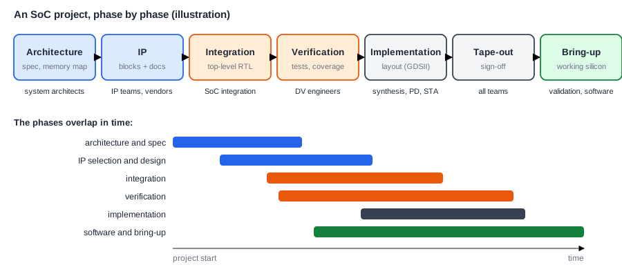
Architecture
Architecture turns product requirements into a system spec: which blocks the chip has, how they connect, the memory map, the clocks and power domains, and the performance, power and area budgets. Its output is a document, plus models that predict whether the design will meet its targets. From Use Cases to Requirements and The System Architecture Spec cover this phase.
IP
IP (intellectual property) is the industry's word for a reusable block design. Most blocks of an SoC come from earlier projects or from outside vendors: processor cores, interconnects, memory controllers, USB or PCIe controllers and their PHYs, the analog circuits that drive the pins. New blocks are designed only where nothing suitable exists or where the block is what makes the product better than its competitors. Each IP arrives with its RTL (the hardware description in Verilog or SystemVerilog), documentation, and usually a verification environment.
Integration
Integration builds the top level: the RTL module that instantiates every block and connects buses, clocks, resets, interrupts and pins, and implements the memory map in the interconnect's address tables. A large SoC's top level has hundreds of thousands of connections, so much of it is generated by scripts from the spec.
Verification
Verification checks that the RTL does what the spec says, before anything is manufactured. Each block is verified alone first, then the whole SoC, usually with C programs running on the processor in simulation together with verification components that drive and check the interfaces. Verification typically takes the largest share of the engineering effort on a chip. The SoC Verification tutorial covers it.
Implementation
Implementation turns the RTL into a physical layout: synthesis into logic gates, floorplanning, placement, clock tree, routing, and sign-off checks of timing, power and manufacturing rules. The Physical Design tutorial follows the flow step by step.
Tape-out and Bring-up
Tape-out is the moment the final layout is sent to the foundry, which makes the photomasks and starts manufacturing; the name dates from when layouts were shipped on magnetic tape. A few months later, the first chips return, and bring-up begins: the validation team runs the first programs on real silicon, software teams finish firmware and drivers, and the chip is characterized across voltage, temperature and manufacturing variation.
The Teams and Their Hand-Offs
Each phase is owned by a team, and each team works from what another team delivered:
| Team | Receives | Delivers |
|---|---|---|
| System architects | product requirements, use cases | system spec, memory map, budgets |
| IP teams and vendors | block requirements | RTL, documentation, block test environments |
| SoC integration | spec and IP | top-level RTL, register maps |
| Design verification (DV) | spec and RTL | tests, coverage results, bug reports |
| Implementation (synthesis, PD, STA) | RTL and timing constraints | layout, timing and power reports |
| Validation and software | silicon, spec | working chip, firmware, drivers |
The most expensive problems appear at these hand-offs. A wrong address in the memory map, an interrupt that two documents describe differently, a reset that one block expects to be synchronous and another asynchronous: none of these is a bug in any single block. They come from mismatched assumptions between teams, which is why so much SoC verification is about the connections.
Quick Check
Q: A UART block passes all its own tests, but in the SoC it never sends anything. Which team's work is most likely at fault, and why?
Show Answer
Integration. A block that works alone but not in the system is most often connected wrongly: a missing select signal, a wrong address window, or its output not reaching the pin. Integration bugs live in the connections between blocks.
Bugs That Appear Where Blocks Meet: Three Real Cases
Even a very small SoC produces the kind of bugs that SoC projects are organized to catch. These three came from one small RISC-V design. Each block had passed its own tests, and each bug appeared only at a hand-off.
Case 1: Found by Implementation
The interconnect and the APB bridge each contain a small function that decides which subordinate owns an address. Written with a return statement, both simulated correctly in two different simulators. When the blocks were handed to synthesis, the synthesis tool rejected the code: it did not support return inside those functions. The fix was trivial, assigning the result to the function name instead, but no amount of simulation would have found it. Simulation and synthesis tools accept slightly different subsets of the language, which is why implementation teams run trial synthesis on RTL long before it is final.
Case 2: Found by a System Test
The UART's STATUS register has a "busy" bit, which software reads to know when all output has gone out. In the first version, busy was 1 only while a byte was actually being sent on the wire, not while bytes were still waiting in the FIFO. The UART's own behavior was consistent, but a program that waited for busy to drop before ending could stop while bytes were still queued, and the last characters of its output were lost. The register map said "busy" without saying exactly what it meant, the hardware and software sides read it differently, and only a test of the whole system, program plus UART, exposed it. The fix made busy include queued bytes, and the spec now says so.
Case 3: Found by Integration
The processor core had passed its regression tests with a memory that answered every access in one cycle. Inside the SoC, accesses over the bus take several cycles, and the core must freeze its pipeline while it waits. In one case, a value that the pipeline was passing directly from one instruction to the next (forwarding) was lost during that freeze, and the next instruction computed with an old value. The core was correct for the memory it had been tested with and wrong for the system it was used in. The fix added a test setting that makes every data access slower; without the fix, four of six test programs failed at just one extra cycle of latency. Since then the core is always tested with slow memory too.
The three cases have something in common: each block was "done" by its own standard. The bugs lived in the assumptions between them, about tool support, about the meaning of a status bit, about memory timing. That is the reason SoC flows put so much effort into integration testing, early trial runs of later phases, and specs that state every assumption explicitly.
Where Does This Matter?
Industry experience is the same at a much larger scale: a large fraction of bugs found late in SoC projects are integration and interface bugs rather than bugs inside blocks. Teams respond with interface checkers on every bus, connectivity checks generated from the spec, and system-level tests that run real software early.
Why the Phases Overlap
Done strictly in order, a project would take far too long, so the phases overlap. Integration starts with early versions of the IP, verification starts as soon as there is a top level to simulate, and the implementation team runs trial layouts on incomplete RTL to find timing and area problems early. Software is written against simulations, emulators (special hardware that runs the RTL thousands of times faster than simulation) and FPGA prototypes long before silicon exists.
Overlap saves months but brings risk: work done on an early version may need to be redone when the spec or the RTL changes. Projects therefore freeze things in stages, each freeze meaning that further changes need formal approval:
| Milestone | What is frozen | Why then |
|---|---|---|
| spec freeze | block list, memory map, interfaces | every team builds on them |
| RTL freeze | the hardware description | final verification and implementation need a stable design |
| netlist and layout freeze | gates and their placement | sign-off checks need a fixed layout |
| tape-out | everything | the masks are made |
A bug found after RTL freeze is not ignored, but it is fixed with an ECO, an engineering change order: a small, carefully controlled change, sometimes made directly in the gate-level netlist so that the layout does not have to be redone. A bug found after tape-out may need new masks and a new manufacturing run, a respin, which costs months and a large sum of money. If possible, it is worked around in software or firmware instead.
The Cost of Finding a Bug Late
The later a bug is found, the more it costs to fix. In architecture, a mistake costs an edit to a document. In RTL, it costs a code change and new tests. After RTL freeze, it costs an ECO and a review. After tape-out, it costs a respin or a permanent software workaround, and possibly a delayed product. This is the economic reason for everything else in this article: architects model before anyone writes RTL, verification starts the day the first RTL exists, implementation runs trial flows early, and software runs on prototypes. Each one moves the discovery of bugs to an earlier, cheaper point.
Quick Check
Q: Case 1 above was found by running synthesis on early RTL. What would have happened if synthesis had run only after RTL freeze?
Show Answer
The bug would have surfaced at the start of implementation, after verification had signed off the frozen RTL. The fix would then have needed an approved change after freeze, re-verification, and schedule time at the worst moment. Trial synthesis found it while changing the RTL was still free.
Common Mistakes
Mistake #1: Treating integration as simple wiring
The integration logic is small, but it holds most of the assumptions between teams: addresses, resets, interrupts, protocols and timing. Plan verification for the connections, not only for each block.
Mistake #2: Waiting for finished IP before starting integration
Starting late compresses verification and implementation into the end of the schedule. Integrate early versions, freeze interfaces first, and update blocks as they mature.
Mistake #3: Leaving software until silicon arrives
Firmware and drivers written only after tape-out leave bugs undiscovered until it is too late to fix them in hardware. Software teams should run on simulations, emulators and FPGA prototypes from early in the project.
Practice Exercise
Challenge: Overlap and Schedule
A simplified project has these phases and durations: architecture 3 months, IP and RTL 8 months, verification 10 months, implementation 5 months, then manufacturing 3 months until silicon is back. (a) How long until silicon if every phase starts only when the previous one ends? (b) Suppose RTL starts after 2 months of architecture, verification starts 2 months after RTL starts and ends 1 month after RTL ends, and implementation starts 4 months before verification ends. How long until silicon now? (c) Name one risk the overlap creates and one practice that controls it.
Hint
For (b), place each phase on a time line in months and find when the last one ends.
Solution
(a) 3 + 8 + 10 + 5 + 3 = 29 months. (b) RTL runs from month 2 to 10. Verification starts at month 4 and ends at month 11 (one month after RTL ends). Implementation starts 4 months before that, at month 7, and takes 5 months, ending at month 12. Silicon is back at month 15, almost half the sequential time. (c) Risk: verification and implementation work on RTL that still changes, so work must be redone. Control: freeze interfaces and the memory map early, and freeze the RTL before final verification and implementation sign-off.
Summary
- An SoC project runs through architecture, IP, integration, verification, implementation, tape-out and bring-up.
- Each phase has an owning team, and the costliest bugs come from mismatched assumptions at the hand-offs.
- Three real bugs from a small SoC were each invisible to their block's own tests: a synthesis-only language issue, a vaguely specified status bit, and a core that failed only with slower memory.
- Phases overlap to save time; spec, RTL and layout freezes, ECOs and early trial runs contain the risk.
- A bug costs more the later it is found, up to a respin after tape-out.
