
DRAM is the main memory of almost every SoC that runs an operating system: gigabytes of storage in separate chips, cheap per bit but slow and full of rules. To use it well, an architect must know how it is organized inside, because the time an access takes depends heavily on what was accessed just before. This article explains how a DRAM cell stores a bit, how cells are organized into banks, rows and columns, what the main timing parameters mean, why refresh is needed, and how the address of a byte is spread over the structure.
12 min read | Intermediate
What You'll Learn
- Explain how a DRAM cell stores a bit and why it needs refresh
- Describe channels, ranks, banks, rows and columns
- Use timing parameters to calculate the latency of different accesses
- Explain how an address is mapped onto the DRAM structure
The DRAM Cell
A DRAM bit is stored as electric charge in a tiny capacitor, reached through one transistor. Charged means 1, empty means 0. That is far smaller than an SRAM cell, which uses six transistors, so DRAM stores many times more bits per square millimeter and costs much less per bit. Memories in a System compares the two.
The capacitor has drawbacks. Its charge leaks away within milliseconds, so every cell must be read and rewritten regularly, which is called refresh. Reading it is destructive: the tiny charge is shared with a long wire, called a bitline, and a sensitive amplifier, a sense amplifier, detects the small change in voltage, then writes the value back. That sensing takes time. These two facts shape everything about how DRAM is used.
DRAM is made in a special process, different from logic, so it sits in separate chips, connected to the SoC through a memory interface of many pins. The SoC side has a memory controller and a PHY, the circuits that drive and sample those pins at high speed.
Rows, Columns and the Row Buffer
Inside a chip, cells form large two-dimensional arrays. A row is a line of cells sharing a wordline. Reading any data first requires an activate command, which opens a whole row: every cell in it is sensed into the sense amplifiers. Those amplifiers together are called the row buffer, and a row is typically a few kilobytes across the chips of a rank.
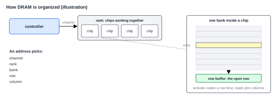
Once a row is open, a read or write command picks a column, a small piece of the row, and transfers it as a short burst over the pins. Further reads from the same row are quick, since the data is already in the row buffer. To use a different row in the same bank, the controller must first close the open one, with a precharge command that writes the row back and prepares the bitlines, and then activate the new one.
So every access is one of three kinds:
- A row hit: the row is already open. Only the column access is needed.
- A row miss to a closed bank: activate, then the column access.
- A row conflict: a different row is open. Precharge, activate, then the column access.
Banks
A DRAM chip has several independent arrays called banks, typically 8 to 16, sometimes grouped into bank groups. Each bank has its own row buffer, and can have a different row open. The controller can activate a row in one bank while reading from another, so their latencies overlap. Banks are DRAM's main source of parallelism, and spreading accesses across them is one of the controller's main jobs.
Ranks and Channels
One DRAM chip is narrow, often 8 or 16 data bits. Several chips are used side by side to fill a wider bus, for example eight 8-bit chips for a 64-bit bus. Chips that work together on every access form a rank. A memory module may have more than one rank, sharing the same wires, but only one can drive the data bus at a time.
A channel is one independent interface, with its own command and data wires. More channels mean more bandwidth: a chip with four channels can run four independent streams of accesses at once. Phone chips usually use several narrow channels, such as 16-bit LPDDR channels, while servers use many 64-bit channels.
Quick Check
Q: Two reads go to the same bank, in different rows, one right after the other. What commands does the second one need?
Show Answer
A precharge to close the first row, an activate to open the second, then the read command. That is a row conflict, the slowest kind of access.
Timing Parameters
A DRAM datasheet lists dozens of timing rules. The three most important give the minimum time between commands:
| Parameter | Meaning | Typical value |
|---|---|---|
| tRCD | activate to read or write (row to column delay) | about 14 ns |
| CL | read command to first data (CAS latency) | about 14 ns |
| tRP | precharge to next activate | about 14 ns |
The values above are rough figures for modern DDR, and they have changed little in nanoseconds for many generations, even as the data rate climbed. That is the reason DRAM latency is often described as a "memory wall": the interface gets faster, but each access still takes about as long. The Memory Hierarchy and Locality explains the consequences.
From these, the latency of each kind of access, ignoring the time on the SoC side, is roughly:
row hit:       CL                  about 14 ns
row miss:      tRCD + CL           about 28 ns
row conflict:  tRP + tRCD + CL     about 42 ns
So a conflict takes about three times as long as a hit, before counting the controller, the interconnect and the clock crossings, which on a real SoC easily add as much again. That is why a load that misses all the caches often takes 80 to 120 ns in total.
Other rules matter too. tRAS is the minimum time a row must stay open, tRC the minimum time between two activates to the same bank, and tFAW limits how many activates may happen in a short window, to keep power under control. The controller must obey all of them.
Data Rate and Bandwidth
Modern DRAM transfers data on both edges of its clock, which is what "double data rate" (DDR) means. A data rate of 6,400 million transfers per second, on a 16-bit channel, gives 6,400 x 2 bytes = 12.8 GB/s per channel at its peak. A burst is usually 8 or 16 transfers, so one read command returns 16 or 32 bytes on a 16-bit channel, or 64 bytes on a 64-bit one, a convenient match for a cache line.
Peak bandwidth is reached only when the data bus is busy every cycle. Row conflicts, bank conflicts, switching the bus between reads and writes, and refresh all leave gaps. Real systems usually sustain 60 to 80 percent of the peak on mixed traffic, and much less on random accesses. Memory Controllers and Scheduling shows how access patterns change this.
Refresh
Every row must be refreshed within a fixed period, commonly 32 or 64 ms. The controller issues refresh commands at regular intervals, often every few microseconds, and each one keeps the affected banks busy for a few hundred nanoseconds. During that time, those banks can't serve requests. Refresh typically takes a few percent of the available time, and more for large, dense chips. It also uses power, even when the memory is idle, which is why phones put DRAM into a self-refresh mode during sleep, in which the chip refreshes itself without the controller.
Where Is This Used?
Different products use different kinds of DRAM. Desktops and servers use DDR4 and DDR5 modules. Phones and laptops use LPDDR, a low-power version soldered close to the SoC, often in the same package. Graphics cards use GDDR, built for very high bandwidth. Accelerators for machine learning use HBM, stacks of DRAM dies placed next to the processor on an interposer, with thousands of data wires. The organization inside is the same for all of them: banks, rows, columns and refresh.
Mapping Addresses to DRAM
The controller must decide which bits of a physical address select the channel, rank, bank, row and column. This choice, the address mapping, has a large effect on performance. A common scheme looks like this, from high to low bits:
| row | rank | bank | channel | column | offset within the burst |
The column bits are low, so a sequential stream stays in one open row for many accesses, which gives row hits. The channel and bank bits are next, so that consecutive rows' worth of data spread over different banks and channels, which gives parallelism. Many controllers also XOR some row bits into the bank bits, so that common access patterns, such as two arrays at addresses that differ by a power of two, don't keep landing in the same bank. This is the same idea as hashing a cache index.
Quick Check
Q: With typical values of 14 ns each for tRP, tRCD and CL, what is the latency of a row hit, a row miss and a row conflict? How much slower is a conflict than a hit?
Show Answer
14 ns, 28 ns and 42 ns. A conflict is three times slower than a hit, before the controller and interconnect add their own delay.
Errors and Reliability
DRAM cells can lose their value through radiation, electrical noise or, in dense chips, interference between neighboring rows. Repeatedly activating one row can disturb its neighbors, a problem known as row hammer, which has been used in security attacks. Systems protect DRAM with ECC, error-correcting codes stored in extra bits, which correct single-bit errors and detect double-bit ones. Servers almost always use ECC, and newer DRAM standards include some ECC inside the chip. Safety and Reliability explains how ECC works.
How DRAM Has Changed
Each new DRAM generation has followed the same pattern. The data rate per pin has roughly doubled, the supply voltage has fallen to save power, and the number of banks has grown, to give the controller more parallelism to hide latency. Bursts have become longer, so that a single command still returns a whole cache line as the bus gets faster. The core timing in nanoseconds has barely moved. So each generation gives much more bandwidth, but hardly any reduction in latency, and the gap between a processor's speed and the time to reach memory keeps growing. An architect therefore plans for DRAM as a high-bandwidth, high-latency resource, and uses caches and on-chip memory to hide the latency.
Common Mistakes
Mistake #1: Treating DRAM latency as fixed
A row hit can be three times faster than a conflict, and refresh adds occasional long delays. Use realistic distributions of latency, not one number, when sizing buffers.
Mistake #2: Quoting only peak bandwidth
Peak bandwidth assumes the data bus is busy every cycle. Real traffic reaches less, and random traffic much less. Plan with a realistic efficiency.
Mistake #3: Ignoring the address mapping
A poor mapping can send a common access pattern to one bank, wasting all the others. Check the mapping against the main access patterns.
Practice Exercise
Challenge: DRAM by the Numbers
An LPDDR channel is 16 bits wide at 6,400 million transfers per second, with bursts of 16 transfers. These numbers are assumptions for this exercise. (a) What is its peak bandwidth? (b) How many bytes does one burst return? (c) If refresh takes 5 percent of the time and row conflicts and bus turnarounds waste a further 25 percent, what bandwidth is left? (d) How many channels are needed to sustain 30 GB/s?
Hint
Peak = transfers per second x bytes per transfer.
Solution
(a) 6,400 million x 2 bytes = 12.8 GB/s. (b) 16 transfers x 2 bytes = 32 bytes. (c) 12.8 x (1 - 0.05 - 0.25) = 8.96 GB/s. (d) 30 / 8.96 = 3.35, so 4 channels.
Summary
- A DRAM bit is charge in a capacitor; it leaks, so it needs refresh, and reading it is slow and destructive.
- Data is organized into channels, ranks, banks, rows and columns; a row must be activated into the row buffer before columns are read.
- A row hit takes about CL, a miss tRCD + CL, and a conflict tRP + tRCD + CL, roughly 14, 28 and 42 ns.
- Banks and channels give parallelism; refresh, conflicts and turnarounds reduce sustained bandwidth.
- The address mapping decides how access patterns spread across banks and channels.
